Difference between revisions of "Layout"
(→Features when designing in PCB mode) |
(→Features when designing in PCB mode) |
||
| (18 intermediate revisions by the same user not shown) | |||
| Line 13: | Line 13: | ||
[[Image:layout.jpg]]<br> | [[Image:layout.jpg]]<br> | ||
By the use of the default settings you see:<br><br> | By the use of the default settings you see:<br><br> | ||
| − | the PCB outline ( | + | Pink: the PCB outline (layer 23)<br> |
| − | the soldering pads (footprints, landmarks) of the | + | Blue: the tracks and soldering pads (footprints, landmarks) of the components on the copper top side (layer 16)<br> |
| − | the | + | Black: the top side position print showing package outlines (layer 21)<br> |
| − | the | + | Black: the top side component names and values(layer 21)<br> |
| − | the | + | Brown: the drills for mounting holes, THT components and vias (layer 24)<br> |
| − | the | + | Red: the tracks and soldering pads (footprints, landmarks) of the components on the copper bottom side (layer 2)<br> |
| − | the position print | + | Cyan: the bottom side position print showing package outlines (layer 7)<br> |
| + | Cyan: the bottom side component names and values (layer 7)<br> | ||
| + | <br> | ||
| + | Layer functions as well as their colors can individually be set. | ||
| + | <br><br> | ||
== Features when designing in [[PCB]] mode == | == Features when designing in [[PCB]] mode == | ||
| − | *permanent back | + | *permanent consistency between schematic and layout (no forth-back annotation required) |
| − | *component | + | *component [[package]]s in the layout can be edited at any time, independently from the component data base |
| − | *2m | + | *2m x 2m (= 78.74" by 78.74") [[Outline|board size]] |
| − | *air wires continually updated in display to aid placing | + | *[[Air wires|air wires]] continually updated in display to aid placing |
| − | *up to 100 layers (copper, solder stop, solder paste, gold etc.) | + | *up to 100 [[Layer|layers]] (copper, solder stop, solder paste, gold etc.) |
| − | *more than one | + | *[[Layer#Layer_colours|color, transparency and hatching]] to be set |
| − | + | *[[Multiple PCBs within one project|more than one PCB in one project]] | |
| − | *any solder pad shapes: circular, octagonal, oblong, polygon | + | *any solder [[pad]] shapes: circular, rectangular, octagonal, oblong, polygon, teardrop |
| − | *extensive SQL component data base containing | + | *extensive [[Component database|SQL component data base]] containing wired and SMD components (steadily growing) |
| − | + | *free access to the component exchange [[Componiverse|COMPONIVERSE®]] | |
| − | *free access to the component exchange [[Componiverse]] | + | *[[Import matching packages (footprints) to the layout|easy assignment and placement of packages]] |
| − | *any width of track, circular track, | + | *automatic placement by configurable [[autoplacer]] |
| − | * | + | *easy manual routing in various [[Signal#Bending_mode|bending modes]] e. g. 45° using a [[grid]] and [[Snap_on_Pin/Pad|snap on boxes]] (snap-on-grid and snap-on-pad and snap-on-track) |
| − | *[[ | + | *[[Track width|any width of track]], circular track, [[Drag|Bézier-curve]], [[spiral]], [[Slider Track|slider track]], [[Meander a track|track meandering]] and [[Differential Pairs|differential pairs]] |
| − | * | + | *custom [[padstack]]s, blind and buried [[via]]s |
| − | * | + | *[[push and shove]]: When manually routing, your current track can push aside existing traces as far as needed (considering spacing rules) |
| − | *configurable | + | *[[auto router]] based on completely new heuristic principles |
| + | **ideal for routing dense conventional or SMD layouts | ||
| + | **bus and fan-out routing | ||
| + | **one-, two- and multilayer routing | ||
| + | **routing of components and pads at any angle | ||
| + | *interface to the external auto router [[Electra|ELECTRA®]] | ||
| + | *[[ground plane]]s calculated in real time | ||
| + | *configurable [[Check project|design rule check (DRC)]] | ||
*PCB generation and routing without schematic | *PCB generation and routing without schematic | ||
| − | *splitting | + | *splitting the schematic off the project later |
| − | *Gerber | + | *[[3D view]] on button click |
| − | * | + | *[[Gerber]] import (e.g. from other design software programs) |
| − | + | *[[Automatic test systems|E testing formats]] <nowiki>*</nowiki>.tgr (Polar Instruments) and <nowiki>*</nowiki>. dif (digitaltest) supported | |
| − | *3D | + | *[[STEP 3D Export|STEP format]] <nowiki>*</nowiki>.stp supported (transfer of 3D data to *other mechanical CAD systems) |
| − | + | *generation of [[panel]]s | |
| − | *generation of | + | *generation of [[Test points|testing points] |
| − | *generation of testing points | + | *[[Select#Selection assistant|selection assistant]] (allows the selection by properties) |
| − | *selection assistant (allows the selection by properties) | + | *[[Molded Interconnect Device (MID)|MID design]]/layout (upon 3D bodies) |
| − | * | + | *[[reverse engineering]]: Underlay layout image, reproduce layout and derive circuit diagram |
| − | * | + | *lots of [[PCB-houses|PCB houses]] accept TARGET <nowiki>*</nowiki>.T3001 files |
| − | * | + | <br> |
| − | * | ||
| − | |||
== [[Assembly Service]] == | == [[Assembly Service]] == | ||
| Line 64: | Line 73: | ||
*add any own parts for assembly (welcome in a bag) | *add any own parts for assembly (welcome in a bag) | ||
*automatic assembly from one(!) piece of PCB | *automatic assembly from one(!) piece of PCB | ||
| − | |||
| − | |||
<br><br><br> | <br><br><br> | ||
Latest revision as of 16:35, 13 May 2019
 |
 Easy layout drawing |
Contents
General
A layout is the binding construction plan of a PCB. In TARGET 3001! it can be edited with or without a schematic.
The expressions layout und PCB or PCB view are often used synonymous in TARGET 3001!, because the same module is meant. The layout is edited in the PCB view. For reaching the PCB layout view in TARGET 3001! click this icon: ![]()
This icon appears in any schematic view. You also might use the [F3] key or the [Shift]+[F3] key. A simple PCB layout might look like this:
A TARGET 3001! - layout
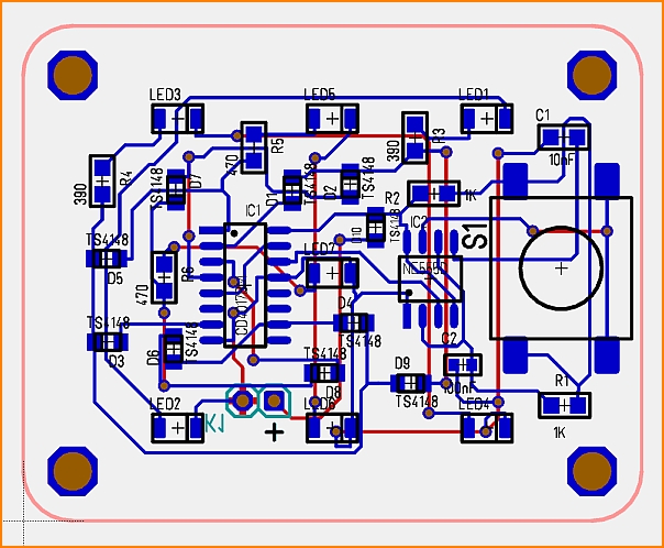
By the use of the default settings you see:
Pink: the PCB outline (layer 23)
Blue: the tracks and soldering pads (footprints, landmarks) of the components on the copper top side (layer 16)
Black: the top side position print showing package outlines (layer 21)
Black: the top side component names and values(layer 21)
Brown: the drills for mounting holes, THT components and vias (layer 24)
Red: the tracks and soldering pads (footprints, landmarks) of the components on the copper bottom side (layer 2)
Cyan: the bottom side position print showing package outlines (layer 7)
Cyan: the bottom side component names and values (layer 7)
Layer functions as well as their colors can individually be set.
Features when designing in PCB mode
- permanent consistency between schematic and layout (no forth-back annotation required)
- component packages in the layout can be edited at any time, independently from the component data base
- 2m x 2m (= 78.74" by 78.74") board size
- air wires continually updated in display to aid placing
- up to 100 layers (copper, solder stop, solder paste, gold etc.)
- color, transparency and hatching to be set
- more than one PCB in one project
- any solder pad shapes: circular, rectangular, octagonal, oblong, polygon, teardrop
- extensive SQL component data base containing wired and SMD components (steadily growing)
- free access to the component exchange COMPONIVERSE®
- easy assignment and placement of packages
- automatic placement by configurable autoplacer
- easy manual routing in various bending modes e. g. 45° using a grid and snap on boxes (snap-on-grid and snap-on-pad and snap-on-track)
- any width of track, circular track, Bézier-curve, spiral, slider track, track meandering and differential pairs
- custom padstacks, blind and buried vias
- push and shove: When manually routing, your current track can push aside existing traces as far as needed (considering spacing rules)
- auto router based on completely new heuristic principles
- ideal for routing dense conventional or SMD layouts
- bus and fan-out routing
- one-, two- and multilayer routing
- routing of components and pads at any angle
- interface to the external auto router ELECTRA®
- ground planes calculated in real time
- configurable design rule check (DRC)
- PCB generation and routing without schematic
- splitting the schematic off the project later
- 3D view on button click
- Gerber import (e.g. from other design software programs)
- E testing formats *.tgr (Polar Instruments) and *. dif (digitaltest) supported
- STEP format *.stp supported (transfer of 3D data to *other mechanical CAD systems)
- generation of panels
- generation of [[Test points|testing points]
- selection assistant (allows the selection by properties)
- MID design/layout (upon 3D bodies)
- reverse engineering: Underlay layout image, reproduce layout and derive circuit diagram
- lots of PCB houses accept TARGET *.T3001 files
Assembly Service
- in cooperation with PCB-POOL®
- calculate the assembly of your board
- define where to purchase the parts
- use standard parts from PCB-Pool® stock
- add any own parts for assembly (welcome in a bag)
- automatic assembly from one(!) piece of PCB
