Layer
General
"Onions have layers. Ogres have layers. We both have layers." (Shrek)
And a PCB layout has layers as well.
A layer in TARGET 3001! is used in the PCB layout view. In schematic view there are no layers. A layer is something like a drawing canvas having a certain function. For example a signal track and a drillhole are drawn each upon a separate layer. The same with the "PCB outline", "Position print" or "Solder mask" and so on. All layers are translucent and lay over each other. So the view in the TARGET 3001! layout is a view from top to the bottom through all layers. Each layer can be faded in or faded out independently whether it carries drawn elements or not.
The principle of how a chosen layer behaves on screen is "view from top to bottom" through all layers:
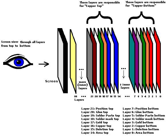
So if you intend to mount a component on the top side and want to solder it from the bottom side, there is no mirroring of pads to the bottom side necessary.
The layer tool
The layer tool is the most important tool within the layout process. In the layout mode TARGET 3001! allows to work on up to 100 layers (0..99), which individually can be edited regarding customized functions. You may assign a function, color, pattern/transparency and a 'related layer'. Such a related layer is called "Assignment". Every layer can be set visible or invisible by ticking the field in front of the desired layer function. Please remember not to set empty (unused) layers visible. This would waste time when refreshing the screen.
![]() This button in the toolbar opens the layer tool.
This button in the toolbar opens the layer tool.
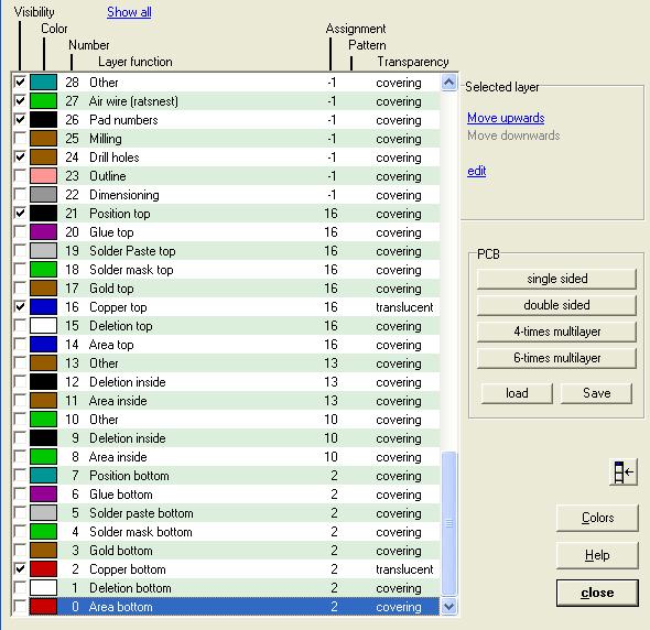
The view of the layer tool at first allows a glance on 29 Layers (0-28), assorted descending. Not all 100 layers can be treated in one view so that a scrollbar on the right hand side is necessary. The default setting shows the layer "Area bottom" at the bottom of the list. Sure you can deviate from this default setting. Later we will see that it is very easy to move a complete layer with all its contents/information/properties upwards or downwards in this list.
Layer functions
Doubleclick a lign of the layer tool in order to edit it's function.
If you place a drawing upon a layer having a certain function, you'll get this function as a result in your board.
The following layer functions can be chosen by default (individual layer functions can be created):
- Copper (bottom, inside, top): Used for solder pads, tracks etc...
- Position (bottom, top): Used for package outline drawings and PCB texts. See also: Component Names and Values Extra. The Gerber format can process it as digital print (resolution up to 0,125 mm). Sikscreen print reaches resolutions up to 0,2 mm. Both techniques work well, silkscreen print is the older standard.
- Deletion (bottom, inside, top): Used for deletions in areas, used especially for automatically generated ground planes.
- Area (bottom, inside, top): Used for automatically generated ground planes.
- Solder mask (bottom, top): Used for the solder mask on copper tracks. This layer is displayed inverse that means any figure you draw upon this layer is free (!) of solderstop, thus solderable.
- Drillholes: Used for drillholes of solder pads, through holes etc...
- Solder paste (bottom, top): Used for the placement of solder paste for smd-components in reflow soldering mode.
- Gold (bottom, top): Used for a partial surface finishing. This for example is used for a gold plating of connectors on a connector card.
- Glue (bottom, top): Used for glue necessary to mount smd-components in wave-soldering mode. All smd component drawings from there individual manufacturers contain a glue-point.
- Dimensioning: Used for outline documentation purposes.
- Outline: Used for PCB outline- and cutout- drawings.
- Milling: Used to give a direct information to milling routers.
- Pad numbers: Used to display the name of individual pins.
- Air wires (ratsnest): Used to display unfinished connections.
- Errors: Used from the design-rule-check to display spacing violations.
- Permissions: Several permission functions.
- Prohibition: Several prohibition functions.
- Component names (bottom, top): Used for having the component names e.g. not on layer "Position..."
- Component values (bottom, top): Used for having the component values e.g. not on layer "Position..."
- Signal names: Used for showing the signal names.
- Other: Used to assign a layer with any other function.
Assignment
The button "Assignment" means that this layer upon which you currently draw refers to a certain copper layer. Each layer can be used as a reference layer for all of the others. If a layer doesn't need an assignment to another layer or it rather does not make sense, please choose -1. By default the area-, deletion- and solder paste layers are assigned either to layer "2, Copper bottom" or layer "16, Copper top". Also see Groundplane.
For example:
Layer "1, deletion bottom" is assigned to layer "2, copper bottom".
That means: all elements drawn upon layer "1, Deletion bottom" lead to deletions on layer "2, Copper bottom".
Layer colours
16 colors are available for the layers: black, light gray, dark blue, light blue, dark green, light green, dark cyan, light cyan, dark red, light red, dark magenta, light magenta, brown, yellow, dark gray and white. Different patterns/transparency can additionally be used to divide layers.
Layers should be dark colored, because selecting (highlighting) a dark colored element leads to a lighter display. It is not convenient to display highlighted elements darker. Also avoid having elements and the window background colored the same. But it´s up to you how you are going to set your colors. But don´t be surprised if you highlight an element and it suddenly fades away because you have generated a "zebra on a zebra crossing".
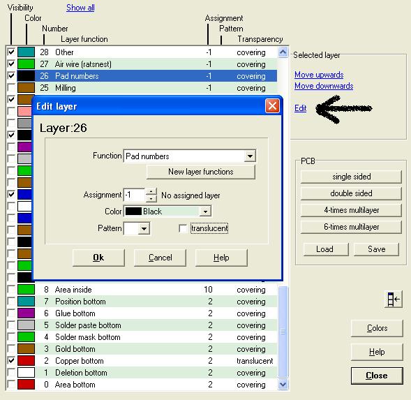
If you doubleclick a layer in the layer tool the dialog "Edit layer" opens. It allows to configurate and administrate all functions a set of layers can achieve.
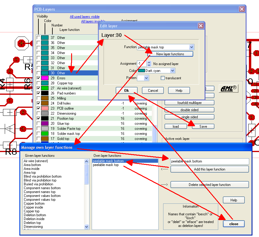
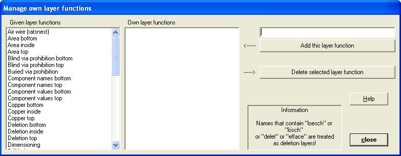
The "New layer functions" button allows to assign your own individual layer functions which then are available for any of the 100 layers. The corresponding Dialog looks like this:
Also the libraries can work with elements having self defined layers. In this case the matching of the name of the layer is very important. "Platin-plating" and "Platinplating" mean different names and will not lead to the expected results.
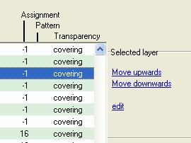
You can move completely all elements of a certain layer to another layer. Highlight e.g. a complete layer by clicking once on this layer in the layer tool dialog. Now press button "move layer upwards" or "downwards". The result is a complete change of a layer. A cross reference to the schematic is done also.
A mini-layer toolbar permanently is displayed on the right edge of screen looking that way:

Visibility
It often makes sense (or it's even necessary) to fade out layers. TARGET 3001! behaves WYSIWYG (what you see is what you get). For printing matters you need to fade out those layers which you don't want to have printed. For fading out a layer, please untick the colored-field in front of the layer function and move in the cursor to the layout again.

Layer 16 (Copper top) in the following picture is not the active drawing layer because the button in front of the layer function is not pressed (no arrow in it). But it is faded in because the tick in the blue field (it defines the color of any element upon this layer) is set. If you wish to fade out the layer 16-elements, please untick the colored field and hover the cursor back into the layout. All blue elements on layer 16 Copper top fade out (they are not deleted).

Please also use buttons "all" to fade in all layers used in your project and "none" to fade out all layers at once:

The layer tool allows to choose predefined sets of layers. On button click you will have a single sided, a double sided, a 4-times or a 6-times multilayer.

You can create your own individual "favourite" sets of layers, save them and load them later in a different project. So you save time by just copying a layer set to a new project.
Administrate individual (customized) layer functions
After you have opened the layer dialog, click M11 upon any layer function and press button "New layer functions". The following dialog will guide you:
Here you can create a new layer function: In the field top right enter the new layer name. By using button: "Add this layer function"...
the existing set of layers can be expanded. The new layer can be seen in the center field. If you close the dialog, the new function is established. Library components can use this new layer function too. The relationship is created by using identical names of the layer functions, not by the use of the layer number. In case you consider MySpecialBerylliumOxideCovering as an appropriate name - remember it well...
The button "Delete selected layer function" has the inverted effect.
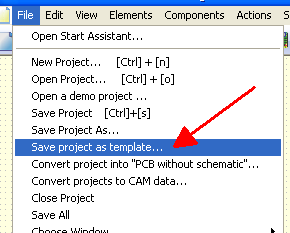
You can also save the layer stack to load it again later on, press button "Save" in the main Dialog "PCB-Layers". You can also save such a project as a template file:
Draw upon a certain layer
In TARGET 3001! the rule is: first select the mode, e. G. "Draw a filled rectangle", afterwards open by the use of the [o]-Key (o for options) the "Options" dialog and select the layer upon which you like to draw.
A different method is clicking M2 on a layer line to activate it for drawing on.

The layer which you currently are drawing on is displayed on top of the screen (the left label).

The other three layer numbers represent the lately used three layers. You can switch them the way you wish.
Change the layer while placing tracks
In case you wish to change the layer during the placement of tracks e. G. from "copper top" to "copper bottom" or the other way round, please press the fullstop key [.] from your keyboard. By this means you place a Via. The chance of the copper layer is done automatically. Changing the copper layers without the use of a via is possible by [Shift]+[.], the colon [:]
Swap layers: Shift all tracks from copper top (Layer 16) to copper bottom (Layer 2) and vice versa
Switch all layers invisible except layer 16, copper top. Now highlight all signal tracks on this layer completely having the Icon
![]() switched on. Find this Icon in the sidebar in section "Settings".
switched on. Find this Icon in the sidebar in section "Settings".
Add tracks to your selection by the use of the [Shift] or [Ctrl] key. After having highlighted all press keyboard key [e] for edition. In the opening dialog "Change tracks" set the layer number from 16 to 2. Press OK. Now your tracks appear on the red layer = 2, copper bottom.
If you shift a track to any non track layer it loses its track properties and ends as a bare line. From this situation the track properties can not be recovered. So you need a third copper layer as a kind of a "interim parking". The editions discover, light, smart und medium have only two copper layers...
Solution: Set a free layer e.g. layer 33 to function "Position top". Now shift all copper tracks from 16 to 33. Now all tracks from 2 to 16 and all "Bridges" from 33 to 2. Lines with a signal upon Positionlayers (like silkscreen) are taken as a bridge and keep the signal.
.
