PCB
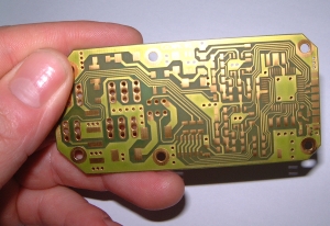
PCB stands for Printed Circuit Board. It is the result of a layout. It is made of a copper coated basic material. The aim is to populate it with electrical components which are connected according to a electrical logic (schematic). The connections are made by leaving copper tracks between connected leads while other copper parts are etched or milled away.

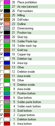
A PCB is the representation of the electrical connections of the pads (footprints) of component packages with solder pads and signal tracks. A PCB layout in TARGET 3001! is made of one or more layers. Layers can have different functions, For example:

Up to 100 layers can be used for a design in TARGET 3001!. You can assign a custom function to any layer. All layers are viewed from the top. Layers with a lower layer number are placed below layers with a higher layer number. Therefore the solder side of the PCB is displayed from the top view (imagine the PCB was made of glass and you look through all layers from the top). An insertion legend print on the bottom layer (7,Position bottom) for example is displayed mirrored on screen.

