Via
What is a via?
A via is a galvanized through hole (plated). It is used only in the layout for connecting top and bottom layer of a PCB at a certain point.

It is used for bringing a track and it's signal to the opposite layer. The image shows the construction principle of a galvanized through hole. It arises when a copper pad gets a drilling with a smaller diameter than the copper itself so that a rest of a copper remains. Then it will be galvanized through. We call the remaining copper a "rest ring".
A via (as well as a through hole pad for wired devices) has a copper flange on top and bottom, this is the copper rest ring. Technically there is no difference between a through hole pad and a via. In most cases the drill of a via is smaller, because no lead of a component needs to run through. If inner layers are inflicted, we talk about a padstack.
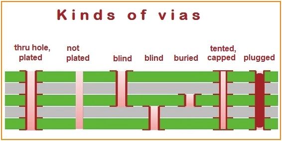
Kinds of vias
How to place a via
|
More? |
You can reach this mode...
by [.] or
by "Place Via" in menu "Elements" or
by "M3" = click the mouse wheel, in "place track" mode
by the tool ![]() under the icon
under the icon ![]() .
.
Leave this mode...
by [ESC] or M12
What you can do:
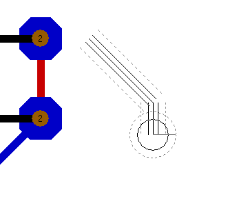
In the following picture we are in the Draw track - mode and have pressed the the keyboard key [.] (full stop) once.

The phantom of the via now can be moved with the cursor. The aura of the via can be seen. Now hover the via to the desired
spot and place it by the use of another [.] full stop or place it by a mouseclick M1.
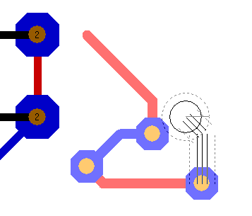
The phantom aura supports you not coming too close to other drawing elements...
How to handle via options
In via mode press [o] for via options prior to placement. It is to select the options for this via and coming ones (see also solder pads).
Vias are visible upon all copper layers (special layer 100) or padstacks (layers 101...254).If a new connection is established between two tracks with different signal names, TARGET 3001! asks you, if you are willing to accept this new connection and which new signal name should be used. If you place a via by M1, TARGET switches immediately into "Draw Tracks" mode.
Press M11 or [o] (for options) in vias mode to select the options for this and future vias (see also solder pads).
Change vias
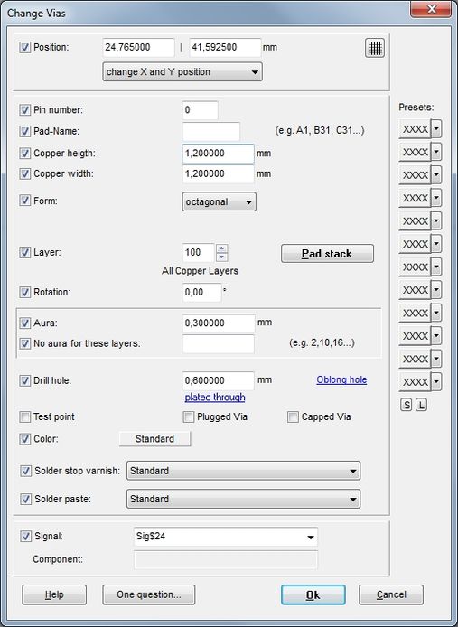
A double click on an existing via opens the following dialog...
What do the Checkboxes in front of properties mean?
Position: Shows realtive or absolute coordinates of the via. Edition allowed.
The button with the grid allows to align the complete grid to this particular point. So in any case this point will be on the grid. So the grid will show an offset which can be turned back in the Grid dialog.
Change X and Y position or only the X-Position or only the Y-Position
Pin number: Is Zero in vias (=0). Giving it a number different to zero makes it a pad.
Pad name: Doesn't play a role in vias. It won't do harm if you give it a name though.
Copper height: Height of the copper landing around the via drill hole
Copper width: Width of the copper landing around the via drill hole
Form: Choose from round, octagonal, rectangle, oblong and polygonal
Layer: 100 means: Through all layers. Upon layer 100 a via is defined.
Padstack: Blind or buried via. Padstacks are to be defined on layers bigger then number 100 also see: Padstack
Rotation: Rotates a via in degree counter clockwise
Aura: Every via as well as every pad generally has an aura (spacing). It gets pushed through as soon as a connection is made by a track. This happens automatically when placing a via during the act of routing.
No aura for these Layers:: If a via shall be connected to a ground plane on a certain layer (maybe an inner layer), its aura gets the value zero on this respective copper layer. The copper layer(s) on which that shall happen is (are) stated here (e.g. 2,10,16.)
Drill hole: Defines the diameter of the drill hole. Note: The inner galvanizing takes away about 10% of the diameter (within reasonable drill hole sizes). So you should use a wider diameter accordingly. Drill holes-put to length- are called "Oblong holes". Define the length here.
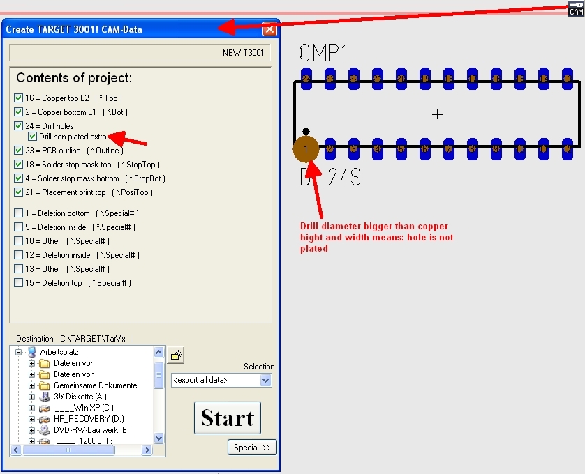
not/plated through: Is copper hight and width smaller than the drill hole diameter a plating through (inner galvanizing) does not take place and vice versa. The mentioning here just announces this.
Test point: This via is a test point
Plugged Via: The via gets a plug made of a conductive or non-conductive material. The aim is to avoid solder agens leaking through or to use the areaof the via drill for soldering. There are various technical alternatives. Speak to your PCB manufacturer regards what you intend to do. TARGET creates each a separate Gerber file representing the vias in question.
Capped Via: The via gets a cap made of a certain kind of varnish. There are various technical alternatives. Speak to your PCB manufacturer regards what you technically intend to do. TARGET creates each a separate Gerber file representing the vias in question.
Color: Standard: Depending on the number of copper layers the rest ring of the via achieves the color of the layer on which it appears. The drill hole achieves the color of the drill layer. The color of the rest ring can be customized.
Solder stop varnish: Select from:
- Standard: For this via the settings of the Gerber driver apply. These settings will be done later during the generation of Gerbers.
- Completely free of solder stop: This via remains solderable and connectable so i won't get in touch with any solder stop agens (example: Testpoint).
- Only drill hole free of solder stop: If liquid solder stop varnish is used the drill hole is protected from the varnish, so that no varnish gets through to the opposite side of the board. That via will not be solderable and not connectable. If your PCB house works with solder resist, this option is redundant.
- Completely covered with solder stop: This via vanishes completely under solder stop varnish.
Solder paste: Won't play a role with vias normally, because vias aren't covered with solder paste like THT pads (elements on layer 100 aren't meant for solder paste application). A via can be "abused" as a SMD test point. Then it might be placed on layer 16 with no drill hole. Now solder paste can be applied or not. As for all SMD pads select from:
- Standard: For this pad the settings of the Gerber driver apply. These settings will be done later during the generation of Gerbers.
- Completely covered with solder paste: The area of this pad exactly will be covered with solder paste.
- Completely free of solder paste: The area of this pad remains free of solder paste.
- Solder paste reduced by X%: Smaller solder paste coating won't overflow the pad's boundaries.
Signal: As far as the via does not have a signal name, select one from the list.
Component: The affiliation of a via to a component is not crucial in most cases. Nevertheless a via can appear like a multi pad in a package. It is in the special situation when two pads lead one signal, maybe within one component. This happens when in a package two pads are generated, having the same pad number. If two pads on the board shall be assigned to only one pin in the schematic, one of both is a pad with one pad number, the other is a via.
the XX-button column to the right: You can save the set of dialog entries to one of the buttons. Press the arrow and rename the button with 2 characters of your choice.
the buttons S and L: allow Saving and Loading of the dialog settings in clear text.
How to change the drill hole size of all vias used in a layout at once?
Drag a highlighting square over your complete layout to highlight all. Now press keyboard key [E] for edit.
In the flashing dialog "Edit the selected elements" tick the box "Vias" and press OK. Now the dialog "Change vias" opens which allows edition of all highlighted vias. Tick the Drill hole box and untick all boxes concerning via properties you do not want to touch. Enter a desired diameter value at "Drill hole" and press OK. Check a via by a double click on it.
Remark: If the drill hole is bigger than the copper around there will remain no copper rest ring. Thus no galvanizing and no contacting will happen. It will come out as a bare hole. So whether a galvanizing through will happen or not is dependant on the existance of a copper rest ring.
How to handle plated an non plated through holes
Maybe you have both kinds of drills and you consider to have them listed separately in Gerber...
Future vias for wired bridges...
... are always free of solderstop varnish and solderpaste.
