Padstack
General
This function is used to create special through holes (vias). Standard vias on layer 100 reach all copper layers and the solder pads of this stack are identical for all copper layers. (Copper top, bottom, inside ...). When creating multi layer PCBs (for example: 4-layer PCB), it is often desired to connect only both of the top layers. This construction shall not create contact or use up space upon both of the bottom layers. To solve this problem, a special plated hole is necessary, called a "blind via" (blind because you can not look through when holding the PCB against the light). It is also possible to construct vias which connect only both inner layers without being visible from the outside. These vias are called "buried vias". Both methods are expensive in production and prone to errors. But TARGET 3001! can create them.
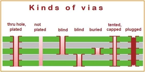
Image: Padstacks are the blind and the buried via.
How to handle Padstacks in TARGET
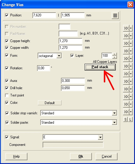
It is possible to resize the solder pads of such a padstack upon each individual layer. There are two ways of opening the dialog for padstack creation: Either you modify an existing via by double clicking on it and entering to the "Padstack" button:
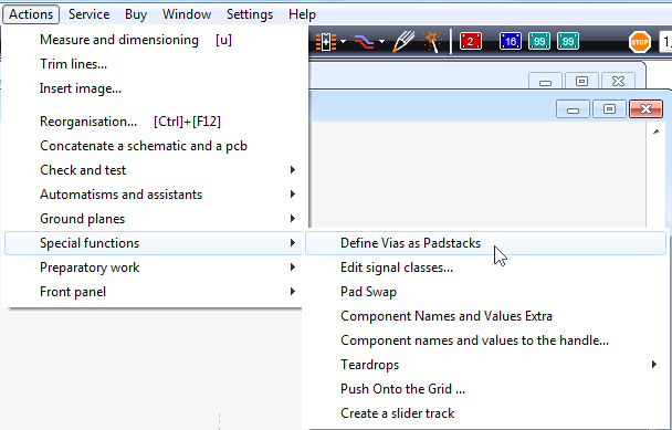
Or you might use the option: "Define Vias as Padstacks" in layout menu "Actions/Special functions/"
In both cases the following dialog appears which allows the creation of padstacks for your current project.
Please note: Changes are executed directly in the project; undo or cancel is not possible.
Please note: In every case you should run the design rule check before producing the PCB!
How to edit a padstack in TARGET
Start with a "New via" for naming a new padstack.
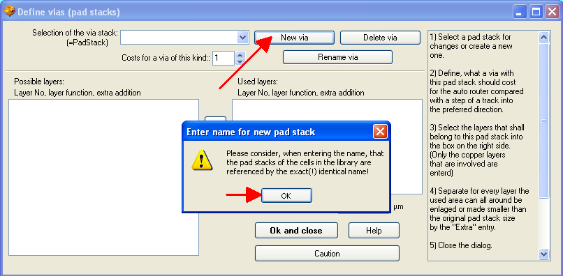
Now name the new padstack in a meaningful way. In our example we want to create a "blind via" which contacts layer 2, copper bottom to the next copper layer, which is 10, "copper inside" so we name it similarly...
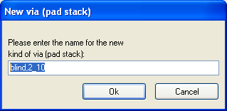
...and define the layers, which shall be touched by the padstack at the end. Please note that padstacks are located on layers 101 upward, independently from their kind of construction.
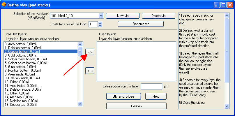
We begin highlighting layer 2 from the layer list on the left. We press the arrow-button which shifts the desired layer to the list on the right side. The list on the right side represents the layers involved in this current padstack.
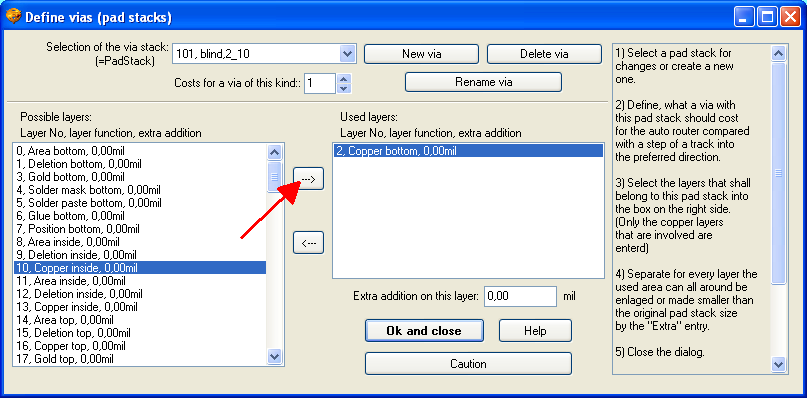
Then we add layer 10, copper inside (if you see layer "10, Other", instead of "10, Copper inside", you need to adjust the layer function). The option "Extra addition on this layer" allows adding or subtracting copper for technical reasons. For instance you will never be able to solder upon an inner layer. Thus for reasons of space a pad on an inner layer can be smaller than on an outer layer. The extra addition on an inner layer must be set negative in this respect.

Now we have created a blind via upon layer 101 named "blind,2_10" connecting the copper bottom layer to the next following inner copper layer. In the dialog "Change Vias" now you are able to choose this kind of padstack at any time...
With a 4 times multilayer the following padstack constructions are thinkable:
- Via 100 = fully drilled through and plated through (normal via).
- Via 2-10 = blind via bottom
- Via 13-16 = blind via top
- Via 10-13 = buried via
- Via 2-10-13 = blind via bottom (seldomly used)
- Via 10-13-16 = blind via top (seldomly used)
- Via 2-13 = blind via bottom (unusual)
- Via 10-16 = blind via top (unusual)
How can I save pads as padstack in a package to the the database?
One thing first: You cannot insert a package with padstacks for a 6-fold multilayer into a double-sided board without padstacks.
Best practice is if you have created a universal blank board with e. g. 6 layers, then define the padstacks and save this blank board as a template. If you then create packages with padstacks, please use this template for the package design. The package now can be exported to the database as usual.
It is always important that the names of the padstacks are identical. This is what TARGET relies on to control padstacks. Padstacks are globally defined within the project like a certain "pattern" and can be used by any soldering pad in the project.
If a padstack used in a certain part is missing in the project, the padstack will be created empty as soon as the component is imported into the project. After that, the padstack can be repaired manually. But that is not the normal procedure. In menu "Actions" under "Special functions" you will find the item "Define Vias as Padstacks".
Padstack drilled completely through
Starting with the V32, you can specify that a padstack is always drilled all the way through, even if it does not contain the outer copper layers. This can save costs because blind and buried vias can be very expensive:
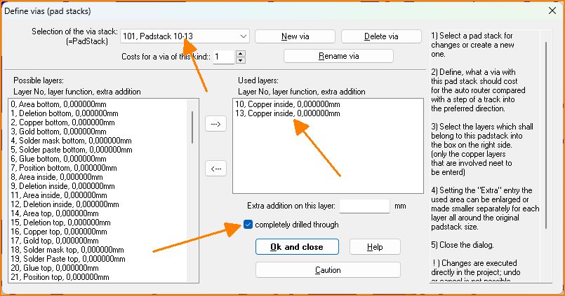
Drill padstack completely through
