Toolbar: Difference between revisions
No edit summary |
No edit summary |
||
| (3 intermediate revisions by the same user not shown) | |||
| Line 132: | Line 132: | ||
[[Image:ReOrganisation.jpg]] [[Reorganisation|Reorganizes]] the whole [[Project|project]] (optimizes the internal database)<br><br> | [[Image:ReOrganisation.jpg]] [[Reorganisation|Reorganizes]] the whole [[Project|project]] (optimizes the internal database)<br><br> | ||
[[Image:Page2.jpg]].[[Image:Page3.jpg]].[[Image:Page4.jpg]] The three | [[Image:Page2.jpg]].[[Image:Page3.jpg]].[[Image:Page4.jpg]] The three recently used [[Schematic|schematic]] pages are shown in this tool. After a selection of a tool button with M1, the [[Schematic|schematic]] page will be opened.<br><br> | ||
[[Image:LayerHistory.jpg]] The layer history <br><br> | [[Image:LayerHistory.jpg]] The layer history as it shows up in a double sided design.<br><br> | ||
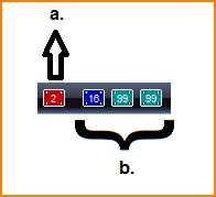
[[Image:Layer2.jpg]] | [[Image:Layer2.jpg]] The left on in the row, see a. above. The currently active [[Layer|layer]] ready to draw on is displayed here. A click with M1 on this tool button allows to [[Select|select]] any other [[Layer|layer]] to draw on [[Layer|layer]]. In "draw track" mode for example it will be possible to [[Select|select]] the desired copper-layer.<br><br> | ||
[[Image:Layer16.jpg]].[[Image:Layer99.jpg]].[[Image:Layer99.jpg]] like b. above. The | [[Image:Layer16.jpg]].[[Image:Layer99.jpg]].[[Image:Layer99.jpg]] like b. above. The three recently used [[PCB]]-layers are shown in this tool. In this constellation only one other layer had been used yet. This is why the others show 99 which means "unused". After a selection of the tool button with M1, the [[Layer|layer]] in question will be activated as the current working [[Layer|layer]]. It also might look like this:<br><br> | ||
[[image: LayerHistory_2.jpg]] Using key [,] comma you can toggle the layer numbers according to the layer history. So it is possible to [[Select|select]] the copper-layer in the "Place track" mode without leaving the cursor position (mouse position).<br> | |||
[[Image:AnzVerbrPins.jpg]] [[Pin|Pins]] used in the current [[Project|project]]. Displayed in the status bar (bottom of screen).<br> | [[Image:AnzVerbrPins.jpg]] [[Pin|Pins]] used in the current [[Project|project]]. Displayed in the status bar (bottom of screen).<br> | ||
| Line 154: | Line 156: | ||
[[Image:Fragezeichen.jpg]] Click on the question mark opens the following [[info]] dialog (e.g.):<br> | [[Image:Fragezeichen.jpg]] Click on the question mark opens the following [[info]] dialog (e.g.):<br> | ||
[[Image:e_FragezeichenDLG.jpg|none]] | [[Image:e_FragezeichenDLG.jpg|none]]<br> | ||
Latest revision as of 15:24, 8 January 2019
For the elements of the Sidebar please have a look there.
The toolbar in schematic view:
![]()
The toolbar in PCB view:
![]()
The toolbar shows the most important TARGET 3001! commands as pictograms. If you are unsecure about the function of a button, please hover the cursor for a short while upon the button without clicking it. A small flag appears showing its purpose. Please note: The toolbar can only be reached using the mouse. Not each of the button functions can be substituted by a menu command. It is not possible, to configure the toolbar individually.
Kinds of tools:
![]() Standard tool: Short click with the left mouse button (=M1): direct function
Standard tool: Short click with the left mouse button (=M1): direct function
![]() Double-tool with an arrow: The standard function of this button can be reached by clicking on the big field left. More detailed functions are available by clicking on the small arrow on the right side of the button.
Double-tool with an arrow: The standard function of this button can be reached by clicking on the big field left. More detailed functions are available by clicking on the small arrow on the right side of the button.
![]() This tool is made of several different functions for the following mouse clicks:
This tool is made of several different functions for the following mouse clicks:
short click with the left mouse button (=M1): function 1
long click with the left mouse button (=M1H): function 2
The description of the function in the small popup window starts also with 3 dots (function 1/... function 2).
Tool functions:
![]() Create a new project. TARGET opens the Sheet.T3001-file and calls it New.T3001. (SheetP.T3001 for a PCB without schematic)
Create a new project. TARGET opens the Sheet.T3001-file and calls it New.T3001. (SheetP.T3001 for a PCB without schematic)
![]() Open an existing project.
Open an existing project.
![]() Left = Save project / Right = Save project as...
Left = Save project / Right = Save project as...
![]() Print the current project view
Print the current project view
![]() Cut and copy highlighted elements to the clipboard. The data will be saved in TARGET-format as well as the Windows-Metafile-Format (WMF). An easy transfer of your schematic- or PCB view without any quality loss to your favourite word processing software (for example: MS-Word) is possible.
Cut and copy highlighted elements to the clipboard. The data will be saved in TARGET-format as well as the Windows-Metafile-Format (WMF). An easy transfer of your schematic- or PCB view without any quality loss to your favourite word processing software (for example: MS-Word) is possible.
![]() Copy highlighted elements to the clipboard
Copy highlighted elements to the clipboard
![]() Paste elements from the clipboard
Paste elements from the clipboard
![]()
![]() Undo / Redo last action
Undo / Redo last action
![]() Change to PCB View. Has a signal or component been highlighted in the schematic view, it will be searched, marked and zoomed in the PCB-view (=cross probe).
Change to PCB View. Has a signal or component been highlighted in the schematic view, it will be searched, marked and zoomed in the PCB-view (=cross probe).
![]() Change to schematic view. Has a signal or component been highlighted in the PCB view, it will be searched, marked and zoomed in the schematic view (=cross probe).
Change to schematic view. Has a signal or component been highlighted in the PCB view, it will be searched, marked and zoomed in the schematic view (=cross probe).
![]() Select any schematic page.
Select any schematic page.
![]() View: The following tools appear:
View: The following tools appear:
![]() Define a scaling factor
Define a scaling factor
![]() Define the grid
Define the grid
![]() Define the colors
Define the colors
![]() Create an additional schematic window
Create an additional schematic window
![]() Create an additional PCB window
Create an additional PCB window
![]() Left = Enter zoom mode / Right = the following zoom tools appear:
Left = Enter zoom mode / Right = the following zoom tools appear:
![]() Zoom out
Zoom out
![]() Zoom in
Zoom in
![]() Refresh the current screen
Refresh the current screen
![]() Center the clicked point in the working area (Pan)
Center the clicked point in the working area (Pan)
![]() Define a scaling factor
Define a scaling factor
![]() Move the whole sheet
Move the whole sheet
![]() Scaling of the circuit fit to screen
Scaling of the circuit fit to screen
![]() Editing-mode: The following tools appear:
Editing-mode: The following tools appear:
![]() Measure distances
Measure distances
![]() Select and highlight a single element
Select and highlight a single element
![]() Delete highlighted elements
Delete highlighted elements
![]() Move highlighted elements
Move highlighted elements
![]() Rotate highlighted elements (with M1)/ ... Define rotation angle (with M1H)
Rotate highlighted elements (with M1)/ ... Define rotation angle (with M1H)
![]() Mirror highlighted elements horizontally (on the vertical axis)
Mirror highlighted elements horizontally (on the vertical axis)
![]() Mirror highlighted elements vertically (on the vertical axis)
Mirror highlighted elements vertically (on the vertical axis)
![]() Edit (change) the highlighted elements
Edit (change) the highlighted elements
![]() Select and rename a signal name
Select and rename a signal name
![]() Left = Insert a component symbol to the schematic/Right = The following tools appear:
Left = Insert a component symbol to the schematic/Right = The following tools appear:
![]() Inserts the remainders (symbols) of a component to the schematic
Inserts the remainders (symbols) of a component to the schematic
![]() Insert reference-symbols to the schematic
Insert reference-symbols to the schematic
![]() Concatenate symbols
Concatenate symbols
![]() Export the selected symbols as one component to the library
Export the selected symbols as one component to the library
![]() Starts the Component database
Starts the Component database
![]() Left = Insert a package-symbol to the PCB/Right = The following tools appear:
Left = Insert a package-symbol to the PCB/Right = The following tools appear:
![]() Export selected elements as a package to a package-library
Export selected elements as a package to a package-library
![]() Starts the Component database
Starts the Component database
![]() Left = Draw signals (schematic)/Right = The following tools appear:
Left = Draw signals (schematic)/Right = The following tools appear:
![]() Draw a signal directly
Draw a signal directly
![]() Draw a signal (first in horizontal direction)
Draw a signal (first in horizontal direction)
![]() Draw a signal (first in vertical direction)
Draw a signal (first in vertical direction)
![]() Draw a signal (first in orthogonal direction)
Draw a signal (first in orthogonal direction)
![]() Draw a signal (first in diagonal direction)
Draw a signal (first in diagonal direction)
![]() Draw a signal being aided by the Schematic router.
Draw a signal being aided by the Schematic router.
![]() .
.![]() .
.![]() .
.![]() Four individually programmable buttons for fixing a default for the drawing of signals. A click on the signal with M1: Call saved signal options. A click on M1H: saves current options to this button
Four individually programmable buttons for fixing a default for the drawing of signals. A click on the signal with M1: Call saved signal options. A click on M1H: saves current options to this button
![]() Edit further signal options
Edit further signal options
![]() Place a junction
Place a junction
![]() Place a bus
Place a bus
![]() Left = Draw track (PCB)/Right = The following tools appear:
Left = Draw track (PCB)/Right = The following tools appear:
![]() Draw a track directly
Draw a track directly
![]() Draw a track (first in horizontal direction)
Draw a track (first in horizontal direction)
![]() Draw a track (first in vertical direction)
Draw a track (first in vertical direction)
![]() Draw a track (first in orthogonal direction)
Draw a track (first in orthogonal direction)
![]() Draw a track (first in diagonal direction)
Draw a track (first in diagonal direction)
![]() .
.![]() .
.![]() .
.![]() Four individually programmable buttons with defaults for the ddrawing of tracks. A click on the track with M1: Call saved track options. A click on M1H: save current options to the button
Four individually programmable buttons with defaults for the ddrawing of tracks. A click on the track with M1: Call saved track options. A click on M1H: save current options to the button
![]() Edit further track options
Edit further track options
![]() Place a via
Place a via
![]() Place a bridge
Place a bridge
![]() Change solder pad into teardrop
Change solder pad into teardrop
![]() Draw a spiral, edit spiral track options
Draw a spiral, edit spiral track options
![]() Draw an air-wire (ratsnest), only for PCB´s without a schematic
Draw an air-wire (ratsnest), only for PCB´s without a schematic
![]() Route Differential pairs
Route Differential pairs
![]() TARGET drawing palette = The following tools appear:
TARGET drawing palette = The following tools appear:
![]() .
.![]() .
.![]() .
.![]() .
.![]() Draw a line, triangle, rectangle, circle and torus
Draw a line, triangle, rectangle, circle and torus
![]() .
.![]() .
.![]() .
.![]() Draw a filled triangle, rectangle, slice and polygon.
Draw a filled triangle, rectangle, slice and polygon.
![]()
![]()
![]() Enter text, Colored field with multiline text, Rectangle to be defined by side lengthes
Enter text, Colored field with multiline text, Rectangle to be defined by side lengthes
![]() .
.![]() .
.![]() Only in schematic-mode: Place a pin, a junction and a bus
Only in schematic-mode: Place a pin, a junction and a bus
![]() .
.![]() .
.![]() .
.![]() Only in PCB-mode: Place solder pads, vias, bridges and Mounting holes.
Only in PCB-mode: Place solder pads, vias, bridges and Mounting holes.
![]() Only in PCB-mode without schematic: Place ratsnest
Only in PCB-mode without schematic: Place ratsnest
![]() .
.![]() .
.![]() Place orientation marks (fiducials)
Place orientation marks (fiducials)
![]() .
.![]() .
.![]() .
.![]() .
.![]() Logic gates according to DIN/IEEE: AND, OR, NOT, XOR, Schmitt-trigger and buffer
Logic gates according to DIN/IEEE: AND, OR, NOT, XOR, Schmitt-trigger and buffer
![]() .
.![]() .
.![]() .
.![]() .
.![]() .
.![]() . Symbols: block-description-fields to create components according to DIN/IEEE
. Symbols: block-description-fields to create components according to DIN/IEEE
![]() .
.![]() .
.![]() .
.![]() .
.![]() .
.![]() . External description-fields to create components according to DIN/IEEE
. External description-fields to create components according to DIN/IEEE
![]() .
.![]() .
.![]() .
.![]() .
.![]() Internal description-fields to create components according to DIN/IEEE
Internal description-fields to create components according to DIN/IEEE
![]() .
.![]() .
.![]() .
.![]() .
.![]() .
.![]() . Other drawing elements
. Other drawing elements
![]() Automatic functions:
Automatic functions:
![]() Measure distances:
Measure distances:
![]() Pad swap|Pin swap (only in schematic-mode)
Pad swap|Pin swap (only in schematic-mode)
![]() Solder pad swap (only in PCB-mode)
Solder pad swap (only in PCB-mode)
![]() Gate swap (symbol swap, only in schematic-mode)
Gate swap (symbol swap, only in schematic-mode)
![]() Starts the autoplacer (only in PCB-mode)
Starts the autoplacer (only in PCB-mode)
![]() Starts the autorouter (only in PCB-mode)
Starts the autorouter (only in PCB-mode)
![]() Opens a dialog to recalculate the ratsnest (only in PCB-mode)
Opens a dialog to recalculate the ratsnest (only in PCB-mode)
![]() Starts the groundplane assistant (only in PCB-mode)
Starts the groundplane assistant (only in PCB-mode)
![]() Check project (schematic and PCB) against parameters you can define and shows resulting violations
Check project (schematic and PCB) against parameters you can define and shows resulting violations
![]() Starts the mixed- mode simulation of the schematic
Starts the mixed- mode simulation of the schematic
![]() Starts the EMC-Analysis of the PCB
Starts the EMC-Analysis of the PCB
![]() Reorganizes the whole project (optimizes the internal database)
Reorganizes the whole project (optimizes the internal database)
![]() .
.![]() .
.![]() The three recently used schematic pages are shown in this tool. After a selection of a tool button with M1, the schematic page will be opened.
The three recently used schematic pages are shown in this tool. After a selection of a tool button with M1, the schematic page will be opened.
 The layer history as it shows up in a double sided design.
![]() The left on in the row, see a. above. The currently active layer ready to draw on is displayed here. A click with M1 on this tool button allows to select any other layer to draw on layer. In "draw track" mode for example it will be possible to select the desired copper-layer.
The left on in the row, see a. above. The currently active layer ready to draw on is displayed here. A click with M1 on this tool button allows to select any other layer to draw on layer. In "draw track" mode for example it will be possible to select the desired copper-layer.
![]() .
.![]() .
.![]() like b. above. The three recently used PCB-layers are shown in this tool. In this constellation only one other layer had been used yet. This is why the others show 99 which means "unused". After a selection of the tool button with M1, the layer in question will be activated as the current working layer. It also might look like this:
like b. above. The three recently used PCB-layers are shown in this tool. In this constellation only one other layer had been used yet. This is why the others show 99 which means "unused". After a selection of the tool button with M1, the layer in question will be activated as the current working layer. It also might look like this:
![]() Using key [,] comma you can toggle the layer numbers according to the layer history. So it is possible to select the copper-layer in the "Place track" mode without leaving the cursor position (mouse position).
Using key [,] comma you can toggle the layer numbers according to the layer history. So it is possible to select the copper-layer in the "Place track" mode without leaving the cursor position (mouse position).
![]() Pins used in the current project. Displayed in the status bar (bottom of screen).
Pins used in the current project. Displayed in the status bar (bottom of screen).
![]() Cancels current action and resets to "Pointer Mode" (= ESC, M12).
Cancels current action and resets to "Pointer Mode" (= ESC, M12).
![]() Shows which variant of assembly you are currently in.
Shows which variant of assembly you are currently in.
![]() Opens the 3D view of the current PCB Layout.
Opens the 3D view of the current PCB Layout.
![]() Opens the dialog for the creation of Gerber data.
Opens the dialog for the creation of Gerber data.
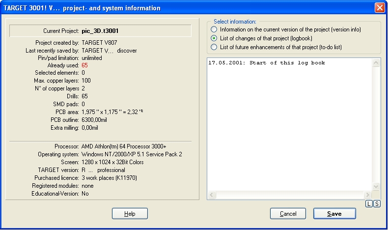
![]() Click on the question mark opens the following info dialog (e.g.):
Click on the question mark opens the following info dialog (e.g.):

On your screen to the right please find the sidebar:
After clicking one of the following tools, a selected (highlighted by M1) signal in pointer- mode will...
![]() ... highlight only the selected signal-segment
... highlight only the selected signal-segment
![]() ... highlight only the selected signal-branch
... highlight only the selected signal-branch
![]() ... highlight only the combined signal-island
... highlight only the combined signal-island
![]() ... highlight the complete signal
... highlight the complete signal
After a selection of the following tools, a move-function with [g] or with [Ctrl] + M1H in pointer-mode, a line caught in its center will...
![]() ... be sharp bended
... be sharp bended
![]() ... bended by an arc of a circle
... bended by an arc of a circle
![]() ... bended by a bezier-curve
... bended by a bezier-curve
![]() If this tool is activated, a selected handle of a component always highlights the whole symbol or package
If this tool is activated, a selected handle of a component always highlights the whole symbol or package
![]() If this tool is activated, each selected element of a figure highlights the whole symbol or package
If this tool is activated, each selected element of a figure highlights the whole symbol or package
![]() If this tool is activated, all elements of a module get highlighted
If this tool is activated, all elements of a module get highlighted
![]() Until V13: This button makes the additional pointer-toolbar be shown permanently.
Until V13: This button makes the additional pointer-toolbar be shown permanently.

