Pad
also see:
- Aura
- SMD
- Solder paste
- Solder stop
- Test points
- Thermal Pads
- Oblong hole
- Used pins/pads
- Via
- Drillhole
- Soldering pad having different auras upon different layers
- Two pads leading one signal
General
A pad in TARGET 3001! is the solderable footprint of a component. A pad is a part of a package, thus an drawing element belonging to the layout.
You can reach this mode in PCB only...
by key [1] (the numeric character 'one' above the alphabetic characters of your keyboard) or
by "Place Pad" in menu "Elements" or
by the tool ![]() under the icon
under the icon ![]()
Leave this mode...
by [ESC] or M12
How to place a pad
Place a free pad by pressing M1 or [Return] at the desired position. Press [o] (options) for pad settings. The ultimate pad used for a package please place by [Return] or [Esc].
Important note: Set the grid to a reasonable value and jump from grid to grid by the use of the "arrow" keys on your keyboard. Place a pad by the key [1] to a desired grid controled point. In Place Pads mode, it is always possible to edit the number and the form of the pins by pressing M11 or [o]:
These free pads are normally used only for the definition of new packages to be saved to the libraries. Subsequential pad numbers are automatically incremented by pressing [1] or M1. Remark: Solder pads whose centre is placed somewhere on a relatively wide track are considered to be connected.
The Pad Options - Change Pads dialog
If you intend to create a new package you will have to arrange pads in a certain pattern. For this reason you need the function Place Pad under the "Drawing functions" icon:
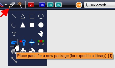
If you press the [O] for Options - key from your keyboard while being in this mode prior to the placement of the pad, you will get the Pad Options dialog. It allows to set the properties of coming pads.
After you have placed a single pad or after you have imported a component package to the layout double click on a pad for editing it. The dialog Change Pads opens. It allows editing a pad after it has been placed. Both dialogs vary only slightly.
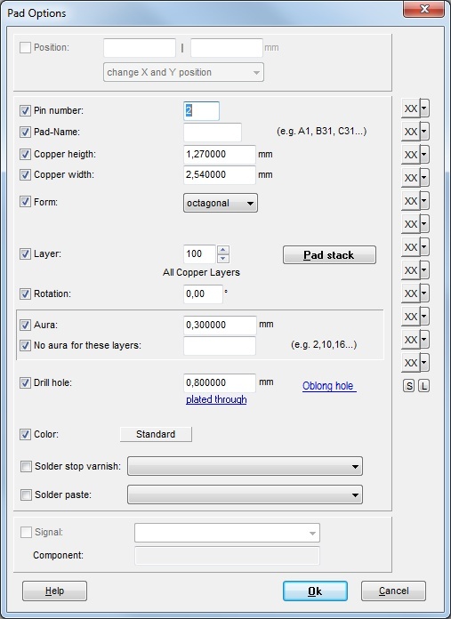
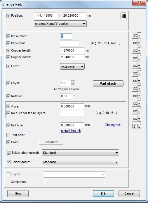
Image: The Pad options and the Change Pads dialog
What is the meaning of the checkboxes in front of properties?
Position: Shows absolute coordinates
change X-and Y-position: If you have highlighted several pads at the same time you can adapt their orientation on one strike.
Pin number: Shows the digit of the pin the pad is related to. If it is Zero, the pad becomes a via.
Pad Name: If the naming of the pins within the package is alphanumerical, (e. g. A1 - A32, B1 - B32, etc.), here you can drop those names. The pad name must be identical to the one of the corresponding pin of the symbol. The pin number must be identical (e. g. pin name of package A1= pin number 1, A32=32, B1=33, B32=65, etc.).
Copper height and width: Shows the dimension of the pad.
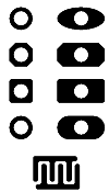
Form: Shows the outline form of the pad. Choose from the following options:
Layer: Defines the layer where the solder pad should appear. For an smd-pad, simply a copper layer number must be entered without a drill hole. For a soldering pad with drillhole, layer 100 (special layer) should be used, which means that the drill hole appears on (= runs through) all copper layers. You can define also padstacks. The according layers therefore are layers 101...254.
Rotation: Shows the orientation of the pin. The cross is the reference point.
Pad aura: The solder pad is also drawn in the corresponding deletion layer. But the outline of the solder pad in the deletion layer is drawn bigger with the value given for the aura. This gives a spacing to other elements. Important when generating ground planes. See also Aura
Drill hole: Sets the diameter of the central drill hole of the pad. For smd-pads the drill hole diameter is 0 (zero). Those ones appear either on layer copper bottom or on copper top solely. You will not find a simple element that represents a simple drill hole as a mounting hole in TARGET. Use the option mounting hole in menu Elements. Alternatively place a via and set its pad size dimensions smaller than the drill hole size. Also you should delete its signal if it has one.
Oblong hole: A pad with a slotted hole. Please have a look here: Oblong hole.
Color: Define color of a pad independently of predefined color. Is color white (R=255, G=255, B=255) chosen, the predefined standard-color is used. If you wish color white although, you need minimal offset from the above mentioned RGB characters (just one point fits).
Solder stop/Solder paste: You can cover one, some or all pads/vias with solder stop or solder paste. Either you use dialog "Special" in Gerber output PCBout to cover all pads/vias or define prior to Gerber data production individual coverings with the pad-properties. Highlight one or more pads/vias and press [e] for edit. Now the dialog change pads opens. The following picture appears:

Tick the box "Solderstop" to cover pads /vias with solder stop or to free them from solder stop or just to fix solder stop to the drill hole. Green in the layout means: here is no solder stop! So this area is solder able. If you don't tick the box or leave setting "Standard" nothing happens right now. That means the decision whether solder stop is used or not can be made later in the Gerber output. If you do nothing there, "Standard" means what your PCB house does as a standard.

Solder paste is to be used when you use SMD components and wish to cover their pads with solder without flooding the complete board with solder.
Define now individual solder paste coverings for one or more pads if desired or leave the "Standard"- setting when the box is ticked. You even might leave the box unticked. The decision to provide solder paste to all or none can be made later in the Gerber output. If you do nothing there, "Standard" means what your PCB house does as a standard.
Signal: Has the pad a signal? If yes, which?
Package: Is the pad part of a package or soldering pattern? If yes, its name is shown here, e.g. IC1, µSOIC8
Rectangular pad having rounded corners
When using lead free solder agens it's possible that little solder balls emerge at the tips of rectangular Pads. They may rip off and stroll alog in your layout and lead to unwanted effects in other locations. To avoid this it is recommended to round the sharp corners of rectangular pads. From TARGET 3001! V15 doubleclick a desired rectangular pad and set the rounding of the corner radius as percentage of its own (shortest) dimension. The following image shows corners of a rectangular Pad rounded by 50% (each 25% to the left and to the right).
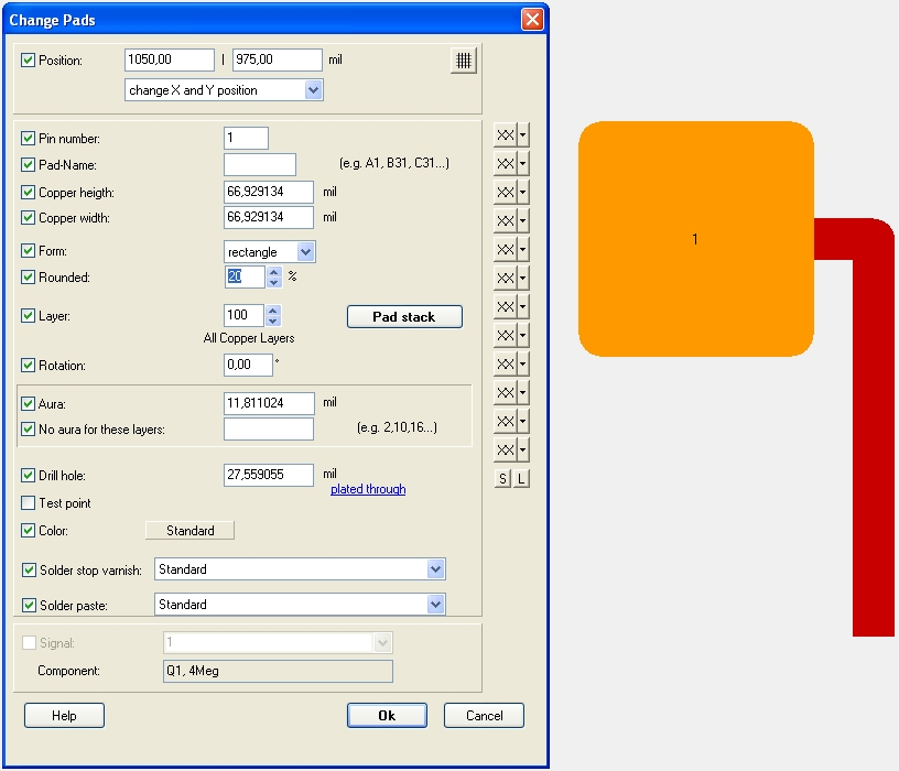
Image: Rectangular pad with rounded corners
From version TARGET 3001! V15 by default rectangular pads have a corner rounding by 20%. You may deviate from this value at your own choice.
Non rectangular pad form
Please also see the article Polygonal pads for to draw free shaped pads (V16 feature).
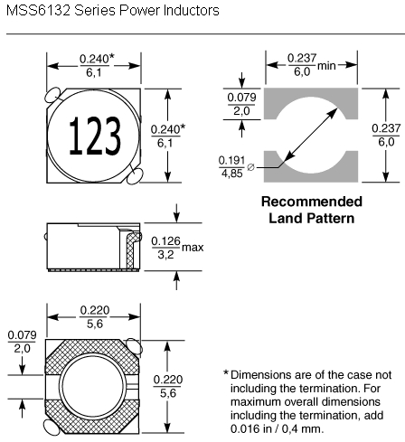
Image: A power inductor having non rectangular soldering areas
In this example the recommended land patterns don't have a rectangular form. You need to draw two rectangular areas on layer 14, Area top. Copy them to layer 18, Solder mask top and 19 Solder paste top. This effects to have them within the solder paste stencil and to keep them free from solderstop varnish. Remember that all in green is free from solderstop. Now place a filled circle on layer 15 Deletion top. In order to make the areas connectible, place each a pad to them at any convenient spot.
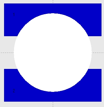
Image: An example how it would look like in TARGET 3001!. At numbers 1 and 2 there is a regular pad behind.
Place pads in a circle
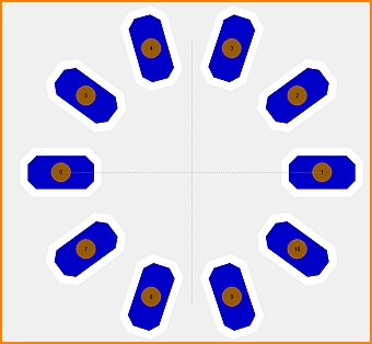
Image: Pads in a circle
10 octagonal pads are to be placed at the same distance on a circle with a radius of 5mm. For this you need auxiliary lines drawn on level 21: a circle with a radius of 5mm and lines at a certain angle to the horizontal, running through the center of the circle and intersecting the circle line at a certain point. The pads are placed on the intersection points of the circle and the lines. First you set the grid very small with [Shift]+[F5], about 0,001mm. The smaller, the easier it is to hit the intersection points later. Now draw a circle with radius 5mm, line width 0.1mm and aura =0. Best around the absolute zero point, which then represents the circle center point.
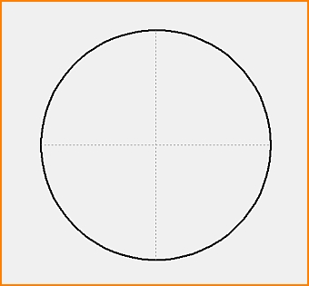
Image: Circle
For 10 pads we divide the full circle of 360° by 10 and therefore have one pad every 36°. Now we create auxiliary lines that are longer than 10mm and that are aligned at angles of 36°, 72°, 108°, 144° and 180°.
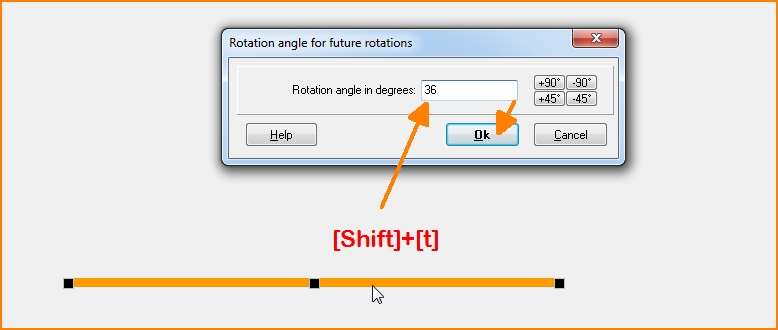
Image: Rotate an auxiliary line with [Shift]+[t] by an angle of 36°. The rotation axis is the mouse pointer position.
TIP: Copy the line with [Ctrl]+[c] and paste it again with [Ctrl]+[v]. With the right mouse button, you can successively rotate them by 36° before placing them.
We place them in the circle so that they run exactly through the center of the circle. The best way to do this is to switch on the X-ray function [#] and concentrate on the "center line".
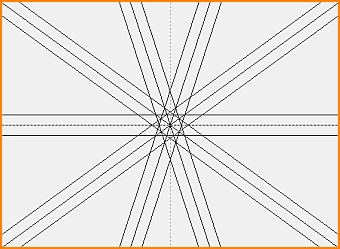
Image: Circle center in x-Ray view [#].
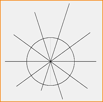
Image: Circle with auxiliary lines in solid view.
Now you place a pad and put it into the clipboard with [Ctrl]+[c]. With [Shift]+[t] you open the dialog "Rotation angle for future rotations" and set an angle of 36°. [Ctrl]+[v] will insert the pad, while M2 will rotate the next pad by 36°. In this way, 10 pads are successively set down, all of which have been rotated by 36°.
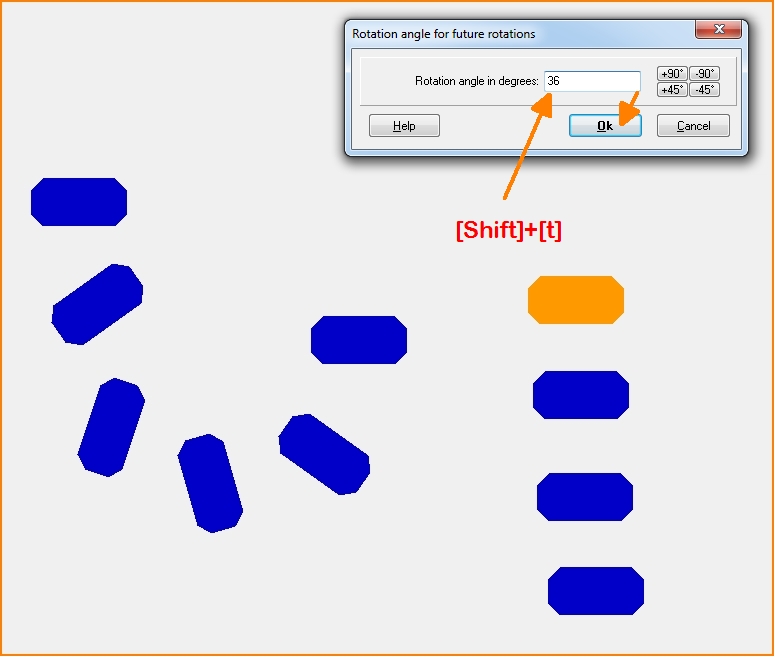
Image: Setting the rotation angle.
Switch to the x-ray view [#] and displace each pad with its center exactly to the intersection line/circle.
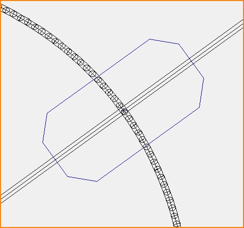
Image: Placement in x-Ray view
As a result we receive the following image:
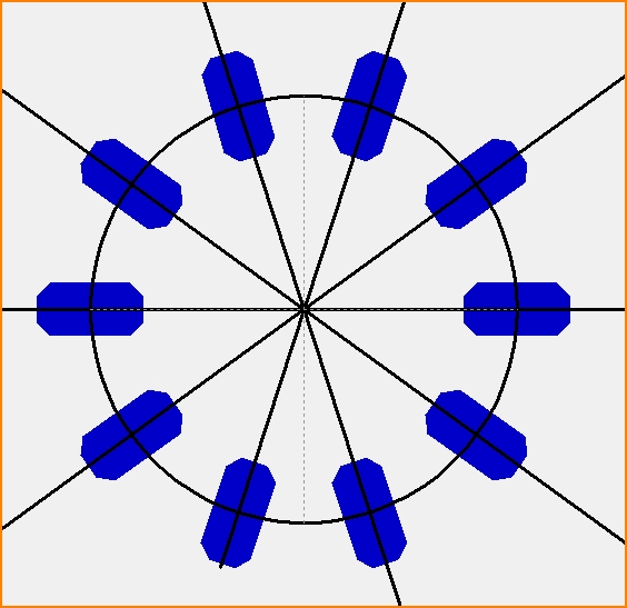
Image: Pads in circle. Now delete the auxiliary lines from layer 21 and fade in all other layers.
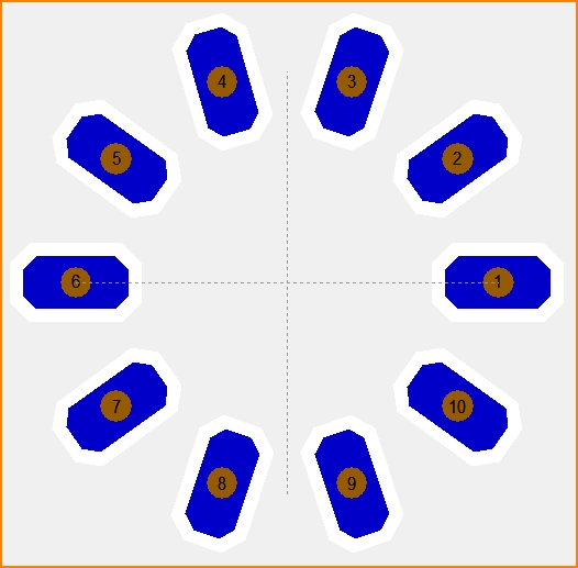
Image: Pads in circle without auxiliary lines. The circle arrangement as a whole of course can also be marked and rotated by any angle.
Working with auxiliary lines can be applied to all geometric forms.
Surface mounted device SMD
Please have a look here: SMD
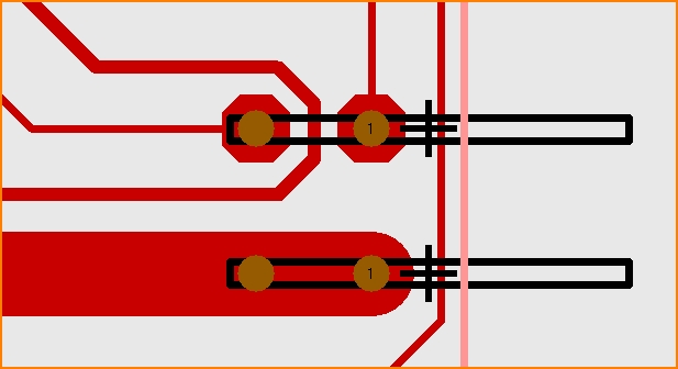
Special: Two pads leading one Signal
also see: Internal connections
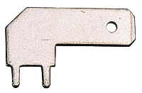
How to construct a connection within a component package, which has only one pin in the schematic, but two pads in the layout? e.g. a clamp which is soldered on two pads but referring to only one logical pin in the schematic. In the package both pads are short-circuited...
In general, there are two situations which need fixing two pads in the layout to only one pin in the schematic:
1) A multitude of pads (at least two) carry the same signal. Both need to be connected - if e.g. GND needs to be connected several times to a processor but only one connection (= one pin) shall be showed in the schematic.
You can exactly superpose several pins in the schematic over each other when creating a symbol. If you later connect
a green signal line to it, all these pins are touched simultaneously. The pads in the layout are created
in a normal way with subsequent pad numbers. For not getting all pin numbers displayed, please set the second
and all further pin numbers invisible.
2) The pads in a package are short-circuited that way that the connection can carry higher current. It also might be used as a bridge.
Place one pin in the schematic having a certain Pin number. In the layout view place more than one pad
all having the same pad number as the pin. TARGET now recognizes that those pads are connected.
When importing this package, TARGET assigns  only one signal to them.
The drawing of such a package is not a problem. Nevertheless the layout of TARGET draws an air wire for two (clamp-internal) connected pads which are recognized as normal connection and processed by the router promptly as track. In fact one would prefer saving this space for other tracks. The "Zero-Ohm-Resistor" -problem is similar. In TARGET the component is constructed having an internal bridge. We are not very happy with this state though...
Pad having a stretched (even rectangular) breakthrough
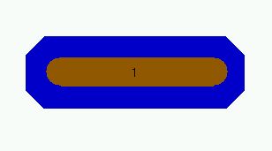
Sometimes data sheets show pads having rectangular breakthroughs (rectangular drillings). Please also see article: "Oblong hole".
De-center the drill of a pad
Double click the pad in question:
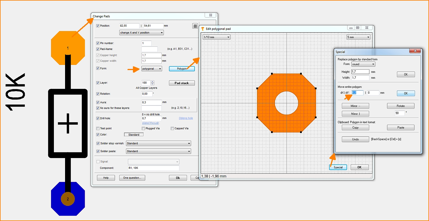
Image: Set off the pad from the drill center. Move the copper dX = 0.2 mm
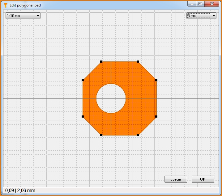
Image: Result of the dialog settings in the pad form preview. Press OK.
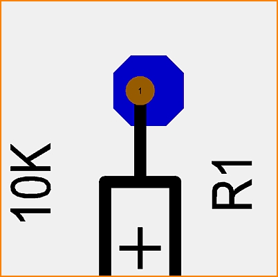
Image: Dialog settings forwarded to the pad in question: Pad set off from the drill center in the layout. So you actually don't de-center the drill but de-center the copper around.
.
