Difference between revisions of "Component"
| (14 intermediate revisions by one other user not shown) | |||
| Line 1: | Line 1: | ||
| − | |||
<br> | <br> | ||
| − | Over 35,000 components are | + | Over 35,000 components are available in your SQL [[Component database]]. There are no libraries. Components can be found by names, descriptions, manufacturers, distributors, parameters and various other attributes.<br><br> <table><tr><td>{{#ev:youtube|-HeDlDCyRrA|300|left|The principle of package drawing}}</td><td> |
| − | |||
*[[Component database]] | *[[Component database]] | ||
*[[Search|Search a component]] | *[[Search|Search a component]] | ||
| + | *[[Create a new component]] | ||
*[[Import a component symbol to the schematic]] | *[[Import a component symbol to the schematic]] | ||
*[[Exchange symbol/package]] | *[[Exchange symbol/package]] | ||
| Line 11: | Line 10: | ||
*[[Edit_component#How_to_modify_an_existing_symbol|How to modify an existing symbol]] | *[[Edit_component#How_to_modify_an_existing_symbol|How to modify an existing symbol]] | ||
*[[Edit_component#How_to_draw_a_symbol|How to draw a schematic symbol]] | *[[Edit_component#How_to_draw_a_symbol|How to draw a schematic symbol]] | ||
| + | *[[Symbol generator|Symbol generator for huge numbers of pins and multi gates]] | ||
*[[Package proposal|Assign a package proposal to a symbol]] | *[[Package proposal|Assign a package proposal to a symbol]] | ||
*[[Component name|Changing the Component Name]] | *[[Component name|Changing the Component Name]] | ||
| Line 21: | Line 21: | ||
**[[Component editor|Only in the current project]] | **[[Component editor|Only in the current project]] | ||
**[[Modify a package in the database|In the database]] | **[[Modify a package in the database|In the database]] | ||
| − | + | *[[Package Generator|Package generator including 3D model]] | |
*[[Edit_component#How_to_draw_a_package|Draw and save a package according to a data sheet]] | *[[Edit_component#How_to_draw_a_package|Draw and save a package according to a data sheet]] | ||
*[[Creation of a 3D Model]] | *[[Creation of a 3D Model]] | ||
| Line 29: | Line 29: | ||
*[[Component Server|The Component Server (up to V13)]] | *[[Component Server|The Component Server (up to V13)]] | ||
*[[Report defective component]] | *[[Report defective component]] | ||
| − | *[[Mirror|Flip a component to the opposite side ]] | + | *[[Mirror|Flip a component to the opposite side]] |
</td></tr></table> | </td></tr></table> | ||
<br> | <br> | ||
| − | [ | + | [//server.ibfriedrich.com/video/e/drawing_a_package/index.html Video: Drawing a package according to a data sheet]<br><br> |
An electronic [[Component|component]] in [[TARGET 3001!]] consists of three main parts: | An electronic [[Component|component]] in [[TARGET 3001!]] consists of three main parts: | ||
*[[Symbol]] for use in the [[Schematic|schematic]] | *[[Symbol]] for use in the [[Schematic|schematic]] | ||
| Line 40: | Line 40: | ||
The component administration is managed in the [[Component database|component data base]]. Further element of a component is one or more [[Simulation]] models. Components can achieve an unlimited number of properties to be used in several internal tasks. In the [[Layout|PCB Layout]] a [[Package|package]] needs to be placed representing the electrical tasks of the schematic symbol (e. g. DIL14 or SO14). There are multiple options to search/find a part.<br><br> | The component administration is managed in the [[Component database|component data base]]. Further element of a component is one or more [[Simulation]] models. Components can achieve an unlimited number of properties to be used in several internal tasks. In the [[Layout|PCB Layout]] a [[Package|package]] needs to be placed representing the electrical tasks of the schematic symbol (e. g. DIL14 or SO14). There are multiple options to search/find a part.<br><br> | ||
| − | <big>'''Open the component data base by the [Ins] key or by the icon [[Image:InsertComponent.jpg|The Import Component icon opens the component data base]]. You will find it middle of the schematic toolbar. Now enter to the search line. | + | <big>'''Open the component data base by the [Ins] key or by the icon [[Image:InsertComponent.jpg|The Import Component icon opens the component data base]]. You will find it middle of the schematic toolbar.'''</big><br><br>Now enter to the search line anything you know about the part in question, e.g. "cd4000".<br><br> |
| − | <br><br> | ||
[[image:database1_e.jpg|none]]<br> | [[image:database1_e.jpg|none]]<br> | ||
'''Component CD4000''': Schematic symbol (fraction), package (= footprint pattern), 3D view. <br><br><br> | '''Component CD4000''': Schematic symbol (fraction), package (= footprint pattern), 3D view. <br><br><br> | ||
| − | In the '''layout view''' of the above IC see the outline of the package in black. This will | + | In the '''layout view''' of the above IC see the outline of the package in black. This will result as the position print as it by default is defined on layer "21, Position print". Blue is the pattern of the soldering landmarks (footprints, pads). They are meant for layer "16, Copper top", which by default is preset in color blue. It is a SMT-part, often being mounted on the assembly side, "Copper top". If you want to have it upon the soldering side (layer "2, Copper bottom") you only need to [[mirror]] it. The pads then will be displayed in red, the default color for "Copper bottom". Sure you individually can set the [[Color|colors]] of each [[Layer|layer]].<br><br> |
| − | Every schematic symbol in TARGET 3001! has a package proposal. You can use it or | + | Every schematic symbol in TARGET 3001! has a package proposal. You can use it or choose a different one. You can use any matching package from the database. During being imported each component gets an individual number. A component can have the name e. g. IC17 (the seventeenth IC in the schematic), R8 (the eighth resistor) and a value (CD4000, 4k7) each can be shown either in schematic or in the layout. |
<br><br> | <br><br> | ||
Latest revision as of 16:02, 20 December 2017
Video: Drawing a package according to a data sheet
An electronic component in TARGET 3001! consists of three main parts:
- Symbol for use in the schematic
- Package (footprint, land pattern) for use in the layout
- 3D-Model for a foto-realistic display of the package as part of the whole design.
The component administration is managed in the component data base. Further element of a component is one or more Simulation models. Components can achieve an unlimited number of properties to be used in several internal tasks. In the PCB Layout a package needs to be placed representing the electrical tasks of the schematic symbol (e. g. DIL14 or SO14). There are multiple options to search/find a part.
Open the component data base by the [Ins] key or by the icon ![]() . You will find it middle of the schematic toolbar.
. You will find it middle of the schematic toolbar.
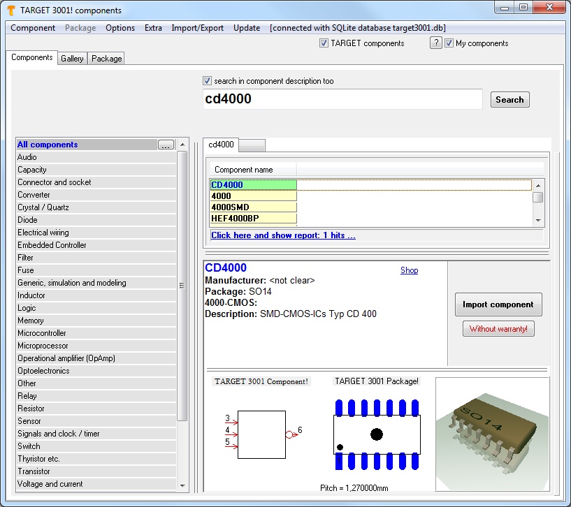
Now enter to the search line anything you know about the part in question, e.g. "cd4000".
Component CD4000: Schematic symbol (fraction), package (= footprint pattern), 3D view.
In the layout view of the above IC see the outline of the package in black. This will result as the position print as it by default is defined on layer "21, Position print". Blue is the pattern of the soldering landmarks (footprints, pads). They are meant for layer "16, Copper top", which by default is preset in color blue. It is a SMT-part, often being mounted on the assembly side, "Copper top". If you want to have it upon the soldering side (layer "2, Copper bottom") you only need to mirror it. The pads then will be displayed in red, the default color for "Copper bottom". Sure you individually can set the colors of each layer.
Every schematic symbol in TARGET 3001! has a package proposal. You can use it or choose a different one. You can use any matching package from the database. During being imported each component gets an individual number. A component can have the name e. g. IC17 (the seventeenth IC in the schematic), R8 (the eighth resistor) and a value (CD4000, 4k7) each can be shown either in schematic or in the layout.
Also see article Menu Components.


