Difference between revisions of "Component"
| Line 40: | Line 40: | ||
The component administration is managed in the [[Component database|component data base]]. Further element of a component is one or more [[Simulation]] models. Components can achieve an unlimited number of properties to be used in several internal tasks. In the [[Layout|PCB Layout]] a [[Package|package]] needs to be placed representing the electrical tasks of the schematic symbol (e. g. DIL14 or SO14). There are multiple options to search/find a part.<br><br> | The component administration is managed in the [[Component database|component data base]]. Further element of a component is one or more [[Simulation]] models. Components can achieve an unlimited number of properties to be used in several internal tasks. In the [[Layout|PCB Layout]] a [[Package|package]] needs to be placed representing the electrical tasks of the schematic symbol (e. g. DIL14 or SO14). There are multiple options to search/find a part.<br><br> | ||
[[image:database1_e.png|none]]<br><br><br> | [[image:database1_e.png|none]]<br><br><br> | ||
| − | '''Symbol CD4000''' ( | + | '''Symbol CD4000''': Schematic symbol (fraction) [[Rests of components|POWER-Symbol]], package (= footprint pattern), 3D view. <br><br><br> |
<br><br> | <br><br> | ||
'''Layout View''' of the above IC. See the outline of the package in black. This will come out as the position print as it by default is defined on layer "21, Position print". Blue is the pattern of the soldering landmarks (pads). They are meant for layer "16, Copper top", which by default is preset in color blue. It is a SMT-part, often being mounted on the assembly side, "Copper top". If you want to have it upon the soldering side (layer "2, Copper bottom") you only need to [[mirror]] it. The pads then will be displayed in red, the default color for "Copper bottom". Sure you individually can set the [[Color|colors]] of each [[Layer|layer]].<br><br> | '''Layout View''' of the above IC. See the outline of the package in black. This will come out as the position print as it by default is defined on layer "21, Position print". Blue is the pattern of the soldering landmarks (pads). They are meant for layer "16, Copper top", which by default is preset in color blue. It is a SMT-part, often being mounted on the assembly side, "Copper top". If you want to have it upon the soldering side (layer "2, Copper bottom") you only need to [[mirror]] it. The pads then will be displayed in red, the default color for "Copper bottom". Sure you individually can set the [[Color|colors]] of each [[Layer|layer]].<br><br> | ||
Revision as of 15:09, 9 July 2014
Over 35,000 components are stored in a SQL Component database. There are no libraries. Components can be found by names, descriptions, manufacturers, distributors, parameters and various other attributes.
Video: Drawing a package according to a data sheet
An electronic component in TARGET 3001! consists of three main parts:
- Symbol for use in the schematic
- Package (footprint, land pattern) for use in the layout
- 3D-Model for a foto-realistic display of the package as part of the whole design.
The component administration is managed in the component data base. Further element of a component is one or more Simulation models. Components can achieve an unlimited number of properties to be used in several internal tasks. In the PCB Layout a package needs to be placed representing the electrical tasks of the schematic symbol (e. g. DIL14 or SO14). There are multiple options to search/find a part.
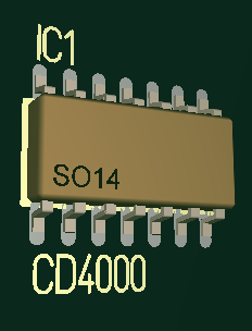
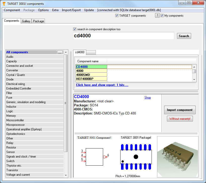
Symbol CD4000: Schematic symbol (fraction) POWER-Symbol, package (= footprint pattern), 3D view.
Layout View of the above IC. See the outline of the package in black. This will come out as the position print as it by default is defined on layer "21, Position print". Blue is the pattern of the soldering landmarks (pads). They are meant for layer "16, Copper top", which by default is preset in color blue. It is a SMT-part, often being mounted on the assembly side, "Copper top". If you want to have it upon the soldering side (layer "2, Copper bottom") you only need to mirror it. The pads then will be displayed in red, the default color for "Copper bottom". Sure you individually can set the colors of each layer.
Every schematic symbol in TARGET 3001! has a package proposal. You can use it or opt for a different one. you can use any matching package from the libraries/database. During being imported each component gets an individual number. A component can have the name e. g. IC17, R8 and a value (CD4000, 4k7) each can be shown either in schematic or in the layout.
You will be able to add a 3D-Model to your part or modify an existing one.
also see article Menu Components


