Menu Actions: Difference between revisions
No edit summary |
No edit summary |
||
| (13 intermediate revisions by the same user not shown) | |||
| Line 1: | Line 1: | ||
'''In schematic view:''' | '''In schematic view:''' | ||
[[Image:e_MenuActionsSchem.jpg|left]] | [[Image:e_MenuActionsSchem.jpg|left]] | ||
[[Measure|Measure and dimensioning]]<br> | |||
[[Line#Trim line|Trim lines]]<br> | |||
[[Insert image]]<br>[[Reorganisation]]<br> | |||
[[Concatenate a schematic and a pcb]]<br> | |||
[[Check project|Check Project]]<br> | |||
[[Symbol / Gate swap|Symbol swap or gate swap]]<br> | |||
[[Pin swap / Pad swap|Pin swap]]<br> | |||
[[Grid|Push Onto the Grid]]<br> | |||
Component names and values to the handle...<br> | |||
[[Alignment Assistant|Launch Alignment Assistant]]<br> | |||
[[Page|Insert Page]]<br>[[Page|Remove Page]]<br> | |||
[[Star shaped ground|Define starshaped signals]]<br> | |||
[[Simulation|Start Simulation]]<br> | |||
[[Block Diagram]]<br> | |||
[[Check Signals|Check all signals]]<br> | |||
[[Signal classes|Edit signal classes]]<br> | |||
[[Molded Interconnect Device (MID)|Prepare MID]]<br> | |||
[[Reverse engineering|Reverse Engineering]]<br><br><br><br> | |||
'''In layout view:'''<br> | '''In layout view:'''<br> | ||
[[Image:E_MenuActionsLay.jpg|left]]<br> | [[Image:E_MenuActionsLay.jpg|left]]<br> | ||
[[Measure|Measure and dimensioning]]<br> | [[Measure|Measure and dimensioning]]<br> | ||
[[Line#Trim line|Trim lines | [[Line#Trim line|Trim lines]]<br> | ||
[[ | [[Insert image|Insert image]]<br> | ||
[[Reorganisation]]<br> | [[Reorganisation]]<br> | ||
[[Concatenate a schematic and a pcb]]<br> | [[Concatenate a schematic and a pcb]]<br> | ||
| Line 21: | Line 39: | ||
[[Breadboard|Breadboard polygon]]<br> | [[Breadboard|Breadboard polygon]]<br> | ||
[[Via_fence|Via fence]]<br> | [[Via_fence|Via fence]]<br> | ||
<br> | [[Signal polygon|Draw signal polygon]] (ground plane = signal polygon)<br> | ||
[[Groundplane|Generate groundplane]]<br> | [[Signal_polygon#Use_the_entire_PCB_area|Entire PCB area]]<br> | ||
Spacing to PCB edge | [[Signal_polygon#Compute_filling|Fill all polygons]]<br> | ||
[[Signal_polygon#Show_or_hide_polygons_upon_visible_layers|Show polygons on visible layers]]<br> | |||
[[Signal_polygon#Retrieve_a_groundplane_not_rendered|Un-fill all polygons]]<br> | |||
[[Signal_polygon#Show_or_hide_polygons_upon_visible_layers|Hide polygons]]<br> | |||
[[Signal_polygon#List_of_polygons|List of polygons]]<br> | |||
[[Signal_polygon#Old_polygons_found|Convert old polygons to V19]]<br> | |||
[[Groundplane|Generate groundplane (versions older than V18)]]<br> | |||
[[Signal_polygon#PCB_edge_spacing|Spacing to PCB edge]]<br> | |||
[[Thermal Pads]]<br> | [[Thermal Pads]]<br> | ||
[[Groundplane#Ground_plane_partitioning|Ground plane partition]]<br> | [[Groundplane#Ground_plane_partitioning|Ground plane partition]]<br> | ||
| Line 29: | Line 54: | ||
[[Padstack|Define Vias as Padstacks]]<br> | [[Padstack|Define Vias as Padstacks]]<br> | ||
[[Signal classes|Edit signal classes]]<br> | [[Signal classes|Edit signal classes]]<br> | ||
[[Pin swap / Pad swap|Pad Swap]] | [[Pin swap / Pad swap|Pad Swap]]<br> | ||
[[Component Names and Values Extra]]<br> | [[Component Names and Values Extra]]<br> | ||
Component names and values to the handle<br> | Component names and values to the handle<br> | ||
| Line 35: | Line 60: | ||
[[Grid|Push Onto the Grid]]<br> | [[Grid|Push Onto the Grid]]<br> | ||
[[Slider Track|Create a slider track]]<br> | [[Slider Track|Create a slider track]]<br> | ||
Convert arcs into line segments<br> | |||
[[Measure|Dimension PCB]]<br> | [[Measure|Dimension PCB]]<br> | ||
[[Panel|Set PCB as a panel]]<br> | [[Panel|Set PCB as a panel]]<br> | ||
Manual assembly<br> | [[Assembly|Manual assembly]]<br><br> | ||
[[Frontpanel]]<br><br> | [[Frontpanel]]<br> | ||
[[Reverse engineering]]<br> | |||
[[fr:Menu Actions]][[de: Schaltplanmenü Aktionen]] | |||
[[category:Menus]] | [[category:Menus]] | ||
Latest revision as of 15:50, 21 August 2018
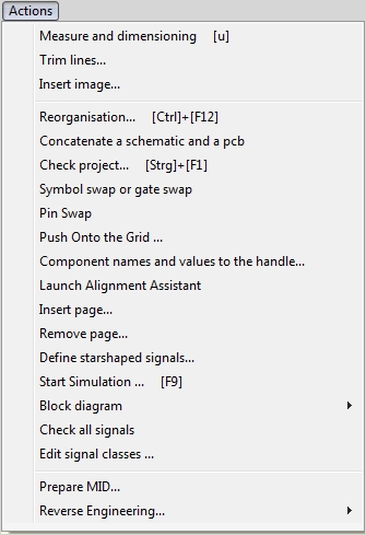
In schematic view:

Measure and dimensioning
Trim lines
Insert image
Reorganisation
Concatenate a schematic and a pcb
Check Project
Symbol swap or gate swap
Pin swap
Push Onto the Grid
Component names and values to the handle...
Launch Alignment Assistant
Insert Page
Remove Page
Define starshaped signals
Start Simulation
Block Diagram
Check all signals
Edit signal classes
Prepare MID
Reverse Engineering
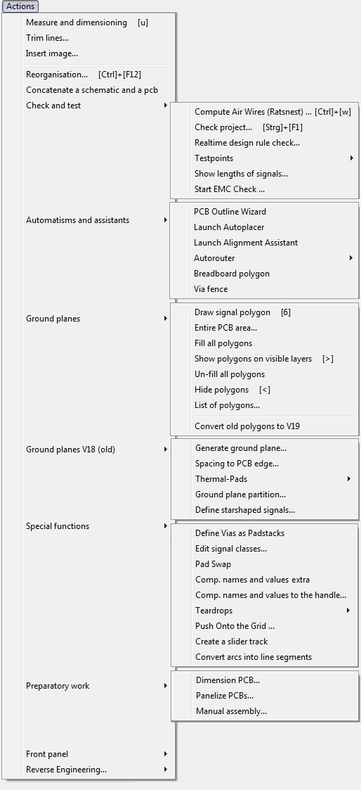
In layout view:

Measure and dimensioning
Trim lines
Insert image
Reorganisation
Concatenate a schematic and a pcb
Compute Air Wires (Ratsnest)
Check project
Realtime design rule check
Test points
Show lengths of signals
Start EMC Check
PCB Outline Wizard
Launch Autoplacer
Launch Alignment Assistant
Autorouter
Breadboard polygon
Via fence
Draw signal polygon (ground plane = signal polygon)
Entire PCB area
Fill all polygons
Show polygons on visible layers
Un-fill all polygons
Hide polygons
List of polygons
Convert old polygons to V19
Generate groundplane (versions older than V18)
Spacing to PCB edge
Thermal Pads
Ground plane partition
Define starshaped signals
Define Vias as Padstacks
Edit signal classes
Pad Swap
Component Names and Values Extra
Component names and values to the handle
Teardrops
Push Onto the Grid
Create a slider track
Convert arcs into line segments
Dimension PCB
Set PCB as a panel
Manual assembly
Frontpanel
Reverse engineering

