Test points
also see:
- Pad
- Aura
- SMD
- Solder paste
- Solder stop
- Thermal Pads
- Oblong hole
- Used pins/pads
- Via
- Drillhole
- Soldering pad having different auras upon different layers
- Two pads leading one signal
General
Test points are needed, if a ready-made layout would not allow the check of it's electrical functions e.g. if you don't have the chance to place measuring sensors to a track without damaging it. A test point upon a signal track must allow access to the signal for measurement purposes.
Example
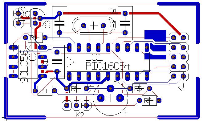
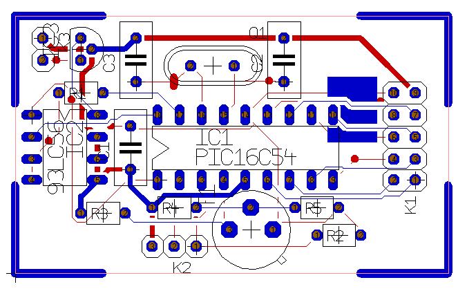
After autorouting of PIC.t3001 the following picture appears:
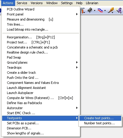
Please find the function "Generate Test Points" in "Menu Actions".
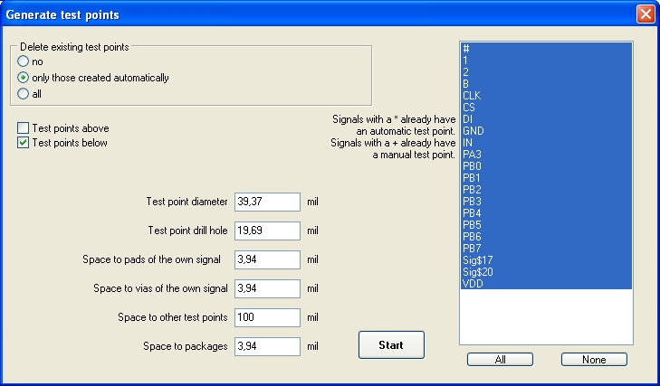
In the opening dialog now enter the settings regarding the dimensions of the test points.
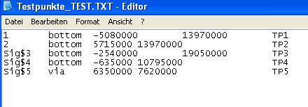
Test points can be generated on "Copper bottom" as well as on "Copper top". When all settings are made, click on the button "Generate test-points". Immediately your text editor opens showing a list of all test points generated (respectively the message "impossible"). The generation of a test point can be denied. Test points can not be generated, if:
- there is not enough space on the track to place a testing point directly upon it
- component packages cover the track
Exception to this second rule: define packages as immune to this rule. This makes sense in those cases when measurements for testing are made prior to the assembly of components on the board. To do so click M1 upon the component, press [e] for edit, press button "Properties" and enter a new line "TESTPOINTS = IGNORE". For our example the list of test points has the following face:
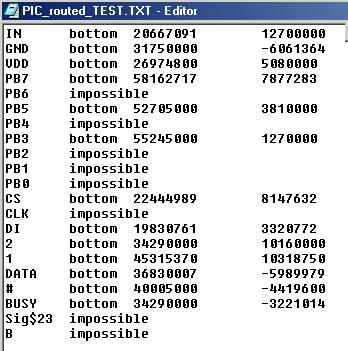
Save ore close the list and view the test points generated:
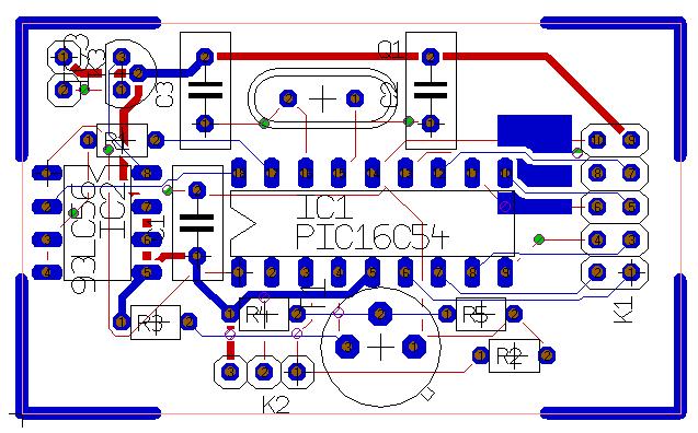
The test points show green in our example, because it is the standard color of layer "Solderstop bottom". Green means: solderstop missing thus test points can be soldered e.g. in HotAirLevelling-technique. The hatched display is the special characteristic of the test points.
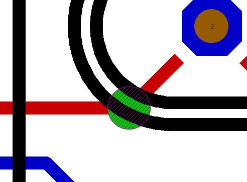
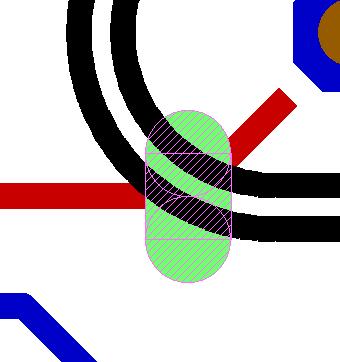
You can also edit test points individually. Hover the cursor over the test point and press [s] for select as often until it flashes and press then [e] for edit. Now enter the desired settings within the flashing dialog. We have defined the above test point as oval, double the height as its width...
The finished layout looks like this:
A test point as a component
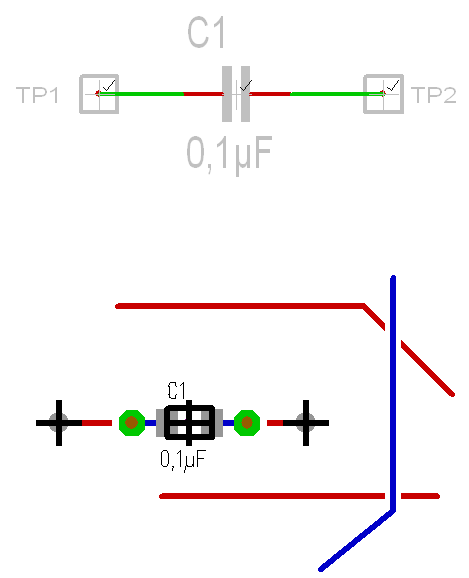
In the component data base you will find a test point like a component - a symbol and a package. Use the search word "testpoint". It is for actively setting a test point in schematic and also in the layout. Later by double click you might edit it according to your wishes. The following image shows two testing points placed in schematic and their correspondings in the layout.
In the layout you will see three further tracks placed by hand: two on copper bottom (red) and one on copper top (blue).
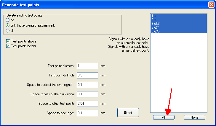
Now we use in menu "Actions" the option "Testpoints/Create testpoints". We will see how both manually placed test points TP1 and TP2 behave compared to the automatically created ones. There will appear a dialog...
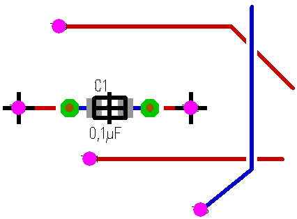
...where we select "All" signals. By this means all testpoints automatically get numbered. After confirmation of the "Start" button the following image shows:
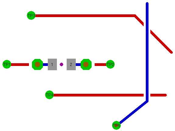
The test points are displayed in pink on layer "28, Testpoints". Their numbering can be seen after switching layer 28, Testpoints, as well as layer 21, Position top invisible:
Lots of testing machines require the PCB being pressed into a needle bed so that the testing procedure is done by the soldering side of the PCB. Technically spoken a test point is some kind of a special via. The blue copper top track needs to be touched from the bottom thus a via is set allowing an electrical contact from below. The test points on copper bottom are relatively unspectacular widenings of the copper track. Testpoints can be controled on layer 102, TESTPOINTS VIA or on layer 101, TESTPOINTS_BOTTOM. Also they appear on layer "Solderstop" in green - being free of solderstop like every thing on this layer which remains free of solderstop. The following image shows the protocol of the automatically generated test points. It also shows the numbering of these test points. It is created into the directory where also your project is saved.
Add the signal name to a test point
A customer asks: "I'd like to create a simple schematic symbol for a test point showing the signal name of the conntacted track automatically. I have created a single pin by the use of key "1" and changed the pin name to "!Signal name". Then I generated the symbol using x and y so that I am able to import it without problems. Unfortunately I see only !SIGNAL, even if i connect it to the track. I have repeated the procedure embedding a text which I hat set to "!Signal name" ...seme result. What am I doing wrong?"
Answer: "Try to change this pin to a "Reference Pin". Use it in the schematic afterwards:"
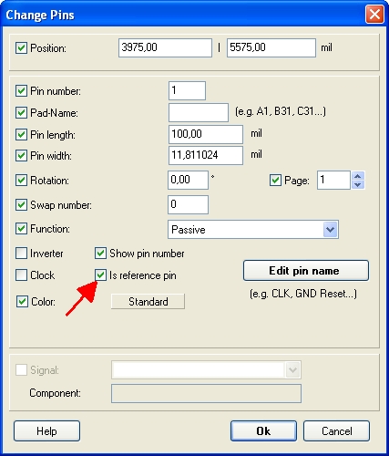
(Image: Doubleclick the pin and enter to this dialog...)


