Drillhole
also see:
- Pad
- Aura
- SMD
- Solder paste
- Solder stop
- Test points
- Thermal Pads
- Oblong hole
- Used pins/pads
- Via
- Soldering pad having different auras upon different layers
- Two pads leading one signal
General considerations
A "Drillhole" is a small hole being drilled into a PCB. It is created either for mounting components by their leads to the PCB or for mounting the whole PCB to an enclosure. In order to create a drillhole simply place a via at the desired location of the PCB without creating any copper tracks.
Click menu "Elements" and there "Place via" or press the full stop [.] key (place via).
However, only "one" drillhole can be created at a time, which means that this method has to be repeated depending on the number of drillholes required. After placing a "Drillhole" (free via), you can configure its settings by M11, which will open a "Change Vias" dialog box. The settings for the drillhole (such as hole diameter, copper height, copper width, aura and signal name) can be altered here.
Important: The layer of a drillhole must be set to 100. This means it passes through all layerss. This way, drill holes will also be visible in the 3D view later on. In the layout view, however, they are displayed on layer "24, drill holes". You can fade them in and out there.
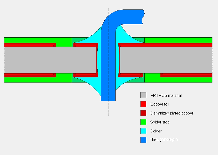
Plated Through hole
The hole diameter depends on the pin diameter. If you have a pin of 0,8 mm, you can take +0,2 mm for the hole. So a final hole of 1 mm would fit. The fact that FR4 is fibered and that galvanizing reduces the hole is normally taken into account by the PCB producer when drilling. If the pin is square instead of round then a factor of 1,4 has to be used for the hole. A square pin has a small square sign instead of a diameter sign associate to it's value.
The pad size (height and width) must be somewhat bigger than the drillhole. At least 0,15 mm around. So add 0,3 mm to the drill diameter to get the pad sizes. If space is available and for manual soldering the pads can be somewhat bigger. The pads do not only have an electric function but a mechanical too. So enlarging the pads leads to stability. On the other hand oversized pads waste PCB space.
The smallest pad form is round (circular), as this shape meets the minimum size rules. An octagonal pad form is ideal for 45° routing, as it is a little bigger than the round pad form but doesn't wast space regarding the routing.
The copper foil on the FR4 material is normally 17 µm = 0,017 mm. The galvanization is about 18 µm giving 35 µm copper at the end. Inside the vias the copper is only 17 µm and less.
The solder stop is around 100 µm = 0,1 mm It can be a silkscreen liquid or a photo resist. The solder stop mask is shown negative in CADs.
The solder mostly is a tin-solder, lead free nowadays. It is coating the pad an the pin and often fills the inner hole completely (capillary attraction).
Mounting hole
"Mounting Holes" are used for mounting a PCB to an enclosure or a housing. Place a mounting hole by menu Elements then "Place mounting drillhole", or by the ![]() (Pen: drawing functions) tool and there choosing File:MountHole.jpg (Place mounting drillhole). Place the mounting hole to the desired location (usually at the corners of the PCB) by clicking M1 or by the [Enter] key.
(Pen: drawing functions) tool and there choosing File:MountHole.jpg (Place mounting drillhole). Place the mounting hole to the desired location (usually at the corners of the PCB) by clicking M1 or by the [Enter] key.
A "Mounting Hole" can be edited by double clicking it with M11 or by selecting it with M1 and pressing the [e] (edit) key. This will open a "Change mounting drillhole" dialog box in which the mounting hole settings can be configured. Mounting Holes, by default are displayed on PCB Layer 24 (Drill Holes Layer), however this dialog shows that the "Layer" setting is set to Layer 100 (All Copper Layers). This is correct as drillholes are placed through all copper layers. If you wish to stabilize the mounting hole by using an annular copper ring, you may do so by setting in this dialog box hight and width of the copper wider than the drilling diameter itself. You aso may assign a signal to it. So if you would have embedded the mounting hole to a groundplane GND, then take away the aura of the mounting drillhole in order to connect it to GND, the mounting drill hole should have signal GND as well. This would avoid alerts later when using the check project function.
To delete a mounting hole, simply select it with M1 and press the [Delete] key.
To leave the "Mounting Hole" mode, press the [Esc] key or click M12.


