Soldering pad having different auras upon different layers
also see:
- Pad
- Aura
- SMD
- Solder paste
- Solder stop
- Test points
- Thermal Pads
- Oblong hole
- Used pins/pads
- Via
- Drillhole
- Two pads leading one signal
General
From version V14 on a soldering pad or a via can achieve different auras on different layers. The main case for using this function is to connect a pad to a certain supply plane by completely embedding it into this plane (i.e. to set it's aura to zero) while the aura remains on other layers. This function will be useful too when working with inner layers or with padstacks. Please find this function in dialog "Change pads".
.
How to embed a soldering pad which leads a supply signal (e.g. GND) on one side completely into a groundplane
Figure 1: Pad No. 1 (arrow) is connected to the groundplane GND (red) by it's signal track.
Figure 1 shows that Pad No. 1 is conneted to the GND Groundplane only by it's signal track. The aura (white) remains for all copper layers. You might increase the connective area by transforming the pad to a "Thermal pad". But what you really want is to reduce the aura of this pad on this current layer to zero, for to embed the pad into the groundplane completely. How to do so? First highlight the soldering pad either with a doubleclick M11 or press keyboard key s for selection as long as the desired pad flashes. Highlight it with [Enter] and open the dialog "Change pads" by the use of key [e] (for edit):
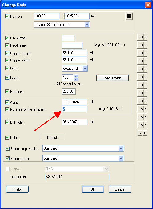
Figure 2: The dialog "Change pads" (from version V14 on).
In this dialog enter to the field "No aura for these layers" the layer number for which layer you like to have the aura set to zero. In our case enter character "2" for copper bottom. You may enter several layer numbers within this field - separated by a comma (z.B. 2,10,16,...). After confirmation with Ok you'll see the result immediately:
Figure 3: Pad No. 1 completely is embedded into the area upon layer 2. It's aura is gone.
.
The aura remains on another supply layer
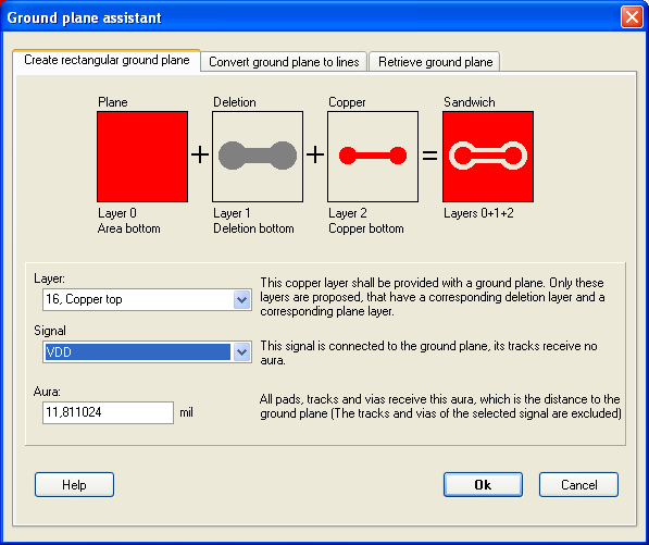
Now we want to check whether the aura of the pad remained on a different suppy layer area. Using the Groundplane assistant we now create another supply area VDD on layer 16, copper top:
Figure 4: The Groundplane assistant in layout Menu Actions
After confirmation with Ok we note that the pads aura on layer 16 VDD (blue) remained.
Figure 5: The pad's aura remains on another layer. 16, copper top in this case.
.
How to embed all VDD pads within the VDD plane on one strike
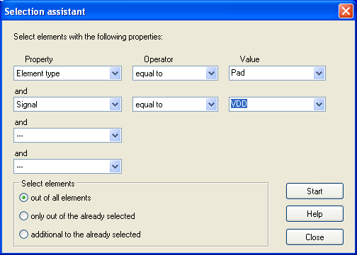
Maybe you wish to embed all solder pads carrying a certain supply signal into the corresponding copper layer. Please first use the Selection assistant in Menu Edit.
Figure 6: The selection assistant showing the search criteria entered.
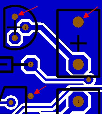
All pads, carrying the desired signal get highlighted.
Figure 7: Highlighted VDD-Pads
Now open the dialog "Change pads" by the use of key [e] (for edit) and use the same procedure as described above. See the result after confirmation with Ok:
Figure 8: VDD Pads embeddet into the VDD plane
.
