Via
also see:
- Pad
- Aura
- SMD
- Solder paste
- Solder stop
- Test points
- Thermal Pads
- Oblong hole
- Used pins/pads
- Drillhole
- Soldering pad having different auras upon different layers
- Two pads leading one signal
What is a via?
A via is a galvanized through hole (plated). It is used only in the layout for connecting top and bottom layer of a PCB at a certain point.

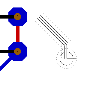
It is used for bringing a track and it's signal to the opposite layer. The image shows the construction principle of a galvanized through hole. It arises when a copper pad gets a drilling with a smaller diameter than the copper itself so that a rest of a copper remains. Then it will be galvanized through. We call the remaining copper a "rest ring".
A via (as well as a through hole pad for wired devices) has a copper flange on top and bottom, this is the copper rest ring. Technically there is no difference between a through hole pad and a via. In most cases the drill of a via is smaller, because no lead of a component needs to run through. If inner layers are inflicted, we talk about a padstack.
How to place a via
You can reach this mode...
by [.] or
by "Place Via" in menu "Elements" or
by the tool ![]() under the icon
under the icon ![]() .
.
Leave this mode...
by [ESC] or M12
What you can do:
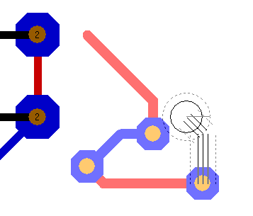
In the following picture we are in the Draw track - mode and have pressed the the keyboard key [.] (full stop) once.

The phantom of the via now can be moved with the cursor. The aura of the via can be seen. Now hover the via to the desired spot and place it by the use of another [.] full stop or place it by a mouseclick M1.
The phantom aura supports you not coming too close to other drawing elements...
How to handle via options
Press [o] for via options. If a new connection is established between two tracks with different signal names, TARGET 3001! asks you, if you are willing to accept this new connection and which new signal name should be used. If you place a via by M1, TARGET switches immediately into "Draw Tracks" mode. Vias are visible upon all copper layers (special layer 100) or padstacks (layers 101...254).
Press M11 or [o] (for options) in vias mode to select the options for this and future vias (see also solder pads).
How to change the drill hole size of all vias used in a layout at once?
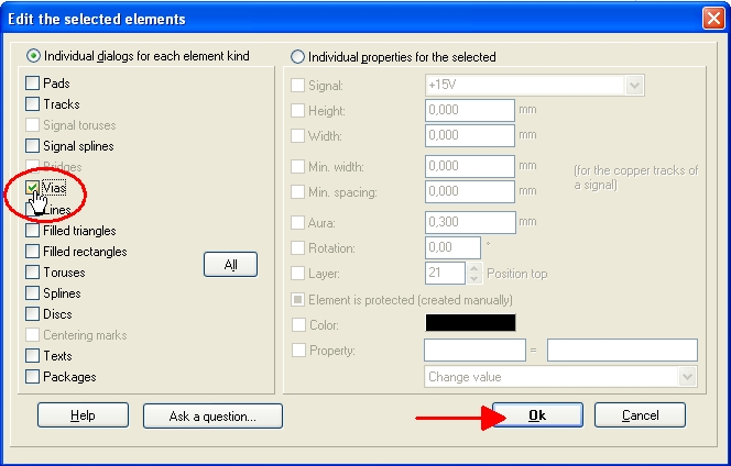
Drag a highlighting square over your complete layout to highlight all. Now press keyboard key [E] for edit.
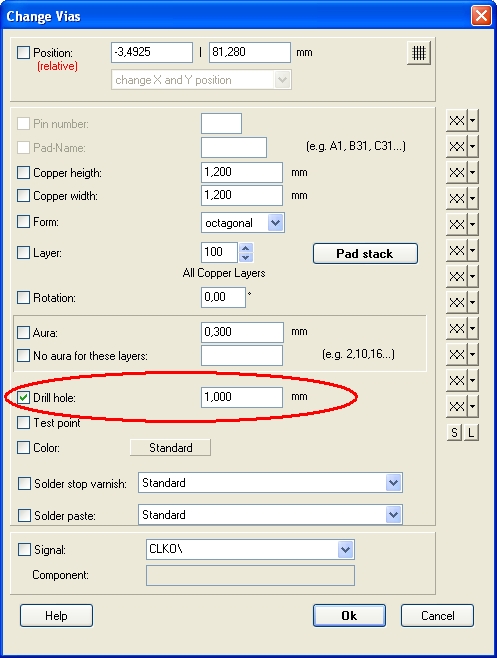
In the flashing dialog "Edit the selected elements" tick the box "Vias" and press OK. Now the dialog "Change vias" opens which allows edition of all highlighted vias. Tick the Drill hole box and untick all boxes concerning via properties you do not want to touch. Enter a desired diameter value at "Drill hole" and press OK. Check a via by a double click on it.
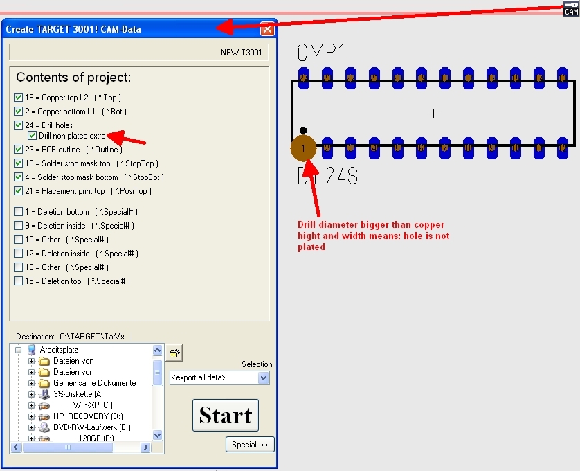
Remark: If the drill hole is bigger than the copper around there will remain no copper rest ring. Thus no galvanizing and no contacting will happen. It will come out as a bare hole. So whether a galvanizing through will happen or not is dependant on the existance of a copper rest ring.
How to handle plated an non plated through holes
Maybe you have both kinds of drills and you consider to have them listed separately in Gerber...
Future vias for wired bridges...
... are always free of solderstop varnish and solderpaste.
