Edit component: Difference between revisions
| Line 182: | Line 182: | ||
Sketch of an SO package according to the datasheet measurements of the package, dimension in inches (millimeters):<br> | Sketch of an SO package according to the datasheet measurements of the package, dimension in inches (millimeters):<br> | ||
[[Image:LTC1392so.jpg|none]]<br><br> | [[Image:LTC1392so.jpg|none]]<br><br> | ||
Lets start with the N8DIP package. For a convenient work with this article it might be good to have | Lets start with the N8DIP package. For a convenient work with this article it might be good to have these two above images printed on paper besides you.<br><br> | ||
1. Open a new project "PCB with schematic" and switch to the empty PCB page [[Image:GotoPCB.jpg]] and select menu '''View/Toolbars/Toolbar "Edit component" visible''' to get the toolbar to the left.<br><br> | 1. Open a new project "PCB with schematic" and switch to the empty PCB page [[Image:GotoPCB.jpg]] and select menu '''View/Toolbars/Toolbar "Edit component" visible''' to get the toolbar to the left.<br><br> | ||
Revision as of 15:50, 15 January 2019
Overview on component drawing (showing the principle)
Create a new component (best practise)
Has anyone else drawn my part already?
Before you start drawing, have a look at COMPONIVERSE, a place to share TARGET parts. Maybe a friend out there has already drawn your part and shares it. Alternatively have a look at each the component portal Ultra Librarian or Samacsys to download CAD data of your desired part in TARGET format.
If you want to draw a component completely new, please start with the package (footprint pattern).
You may use the Package Generator which at the same time provides a 3D model.
As an alternative you may use the Package assistant for devices having a huge amount of leads. You may also draw the component freehand. This article explains in detailed steps, how to create Component Packages, Schematic Symbols, and Reference Symbols.
For 3D models please have a look here: 3D or see the Package Generator.
TARGET 3001! understands a component as the dualism of a component package and one or more schematic symbols. It is recommended to draw the component package first and save it to the database. The reason for this is when you draw a schematic symbol and want to save it to the database, you get asked to assign a package to it which later appears as a "package proposal". Therefore, it is good to have the desired package already available. Later, when the import of an appropriate component package to a layout is required, the above package proposal is optional. That means you can use it but you also can leave it and use a different one, a "free package".
It is recommended that TARGET 3001 users get familiar with the above feature by opening an empty project to try a few examples, and "play around" with this feature. The grid-size should be set 0.635mm = 25mil. It is recommended to have the pin-to-pin distance in the schematic 2.54mm = 100mil = 0.1in (= 4 grid steps). Maybe the quickest way of getting results is to modify existing footprints or symbols. So let's start with this topic.
How to modify an existing component
Let's say you intend to use one of the TARGET 3001! SMD resistors with package 0402 but wish to give it different values. You would just make a copy of it and furnish it with your desired values. This is the way to proceed:
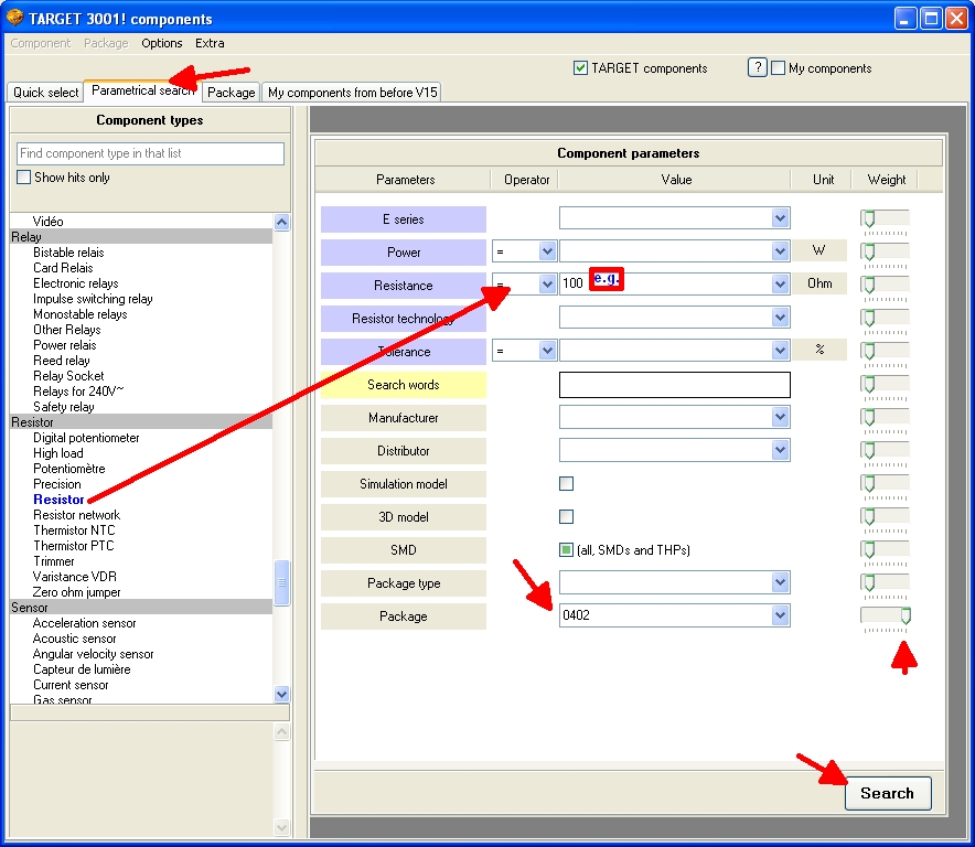
Image1: Start with the "Parametrical search" in the component browser
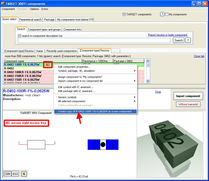
Image2: The one you copy necessarily needn't be a green one. Green means: "All entered parameters match". Regarding mousekeys please follow the link.
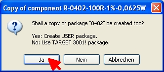
Image3: Yes, you want to copy the package in order to make it a USER package
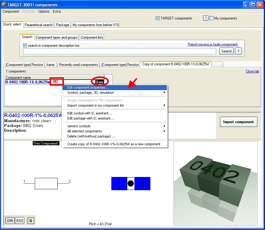
Image4: Within your user copy you now do your settings and amendments.
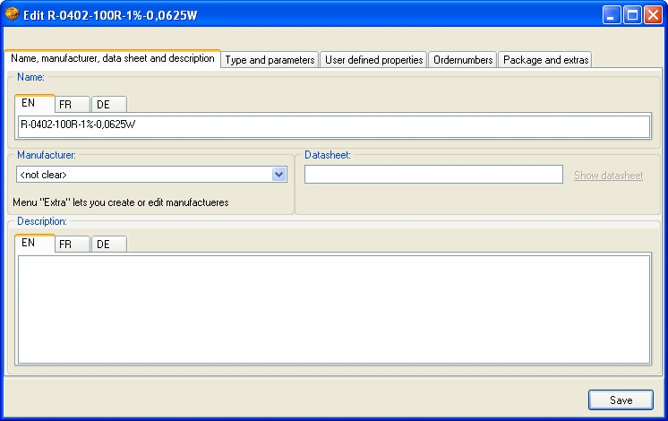
Image5: Go through the tabs to do all your custom entries. Done.
How to modify an existing package
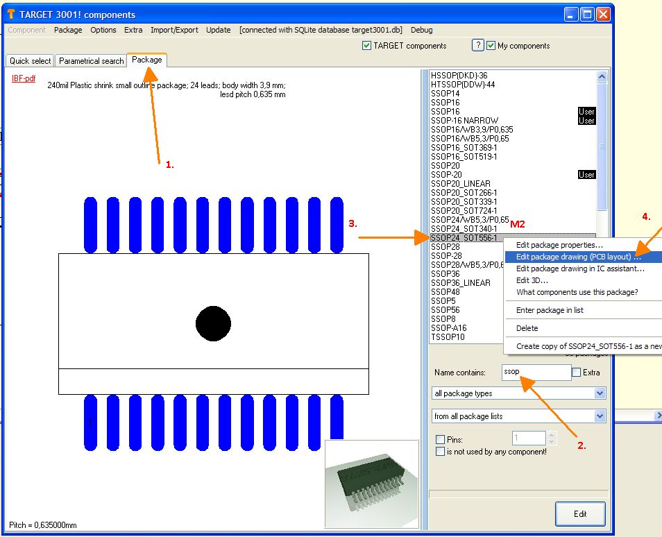
TARGET 3001! allows to modify any package (footprint pattern) separately and save it again as a new (USER-) component. Please press [F2] to start the Component Database browser. Select the tab "Package" (1). Enter "ssop" (2). Right-click M2 on a package name in the list opens a context menu (3). Select "Edit package drawing (PCB Layout)" (4).
Change the component using the drawing functions. Select all, hover the mouse over the old handle cross. Press key [x]. Change the name or other properties. Press OK. The component is saved as a "USER" component now with a black flag. Assure to have "My components" checked with a checkmark on right top of the dialog.
To use the drawing functions while editing an existing component watch this, it is a little more detailed: Guess you are in a design flow and recognize that the Dil_10 you are searching for is missing. Your idea is to modify the Dil_8 from the database to a Dil_10.
1. Open a new "PCB without schematic".
By this means the component browser only shows the packages which contain the footprints. In case you have opened a "PCB with schematic" you first have to switch over to the layout view and select "free package" from the list of package proposals. Don't worry - this works too. The following instructions refer to the situation of a "PCB without schematic".
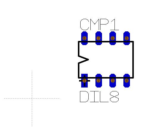
2. Import DIL_8 from the database into the PCB canvas.
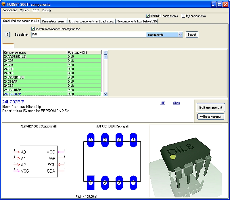
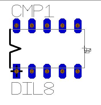
After pressing Edit component you see something similar to the following picture. Choose the format filling scaling factor by key [F7] for a more convenient view.:
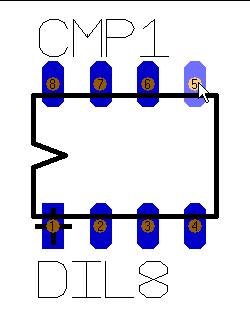
3. Now highlight Pad N° 5 by M1 for copying it by [Ctrl]+[c]. (You might copy any other pad...)
4. Now you have it in your clipboard. Now press [Ctrl]+[v] for pasting it. It's pictogram is fixed to the cursor:
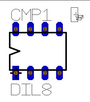
Move it to the left starting from it's initial position to figure out the pitch (distance between the drillings) defined by grid steps. If it does not mantch, please try to set the grid accordingly. Take care for having a grid-move in one step units.
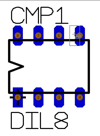
In our example we have a grid of 4 steps. That is the distance we paste the pad to the canvas:
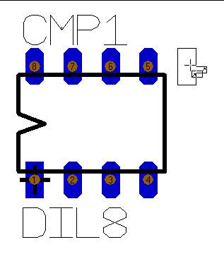
and
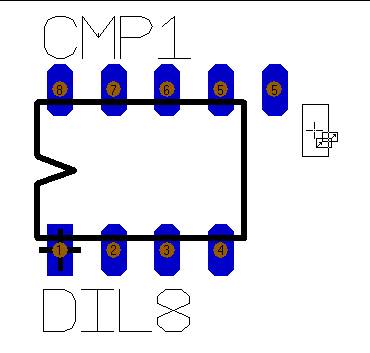
Do the same in the bottom row:
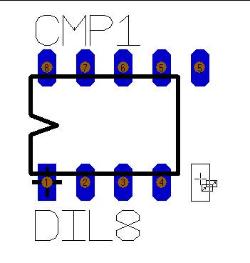
and
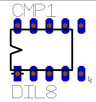
5: Now we have to renumber the pads. Within the lower row the numbering is ok, but in the upper row adjustments have to be made. We double click M11 the upper right pad and have to change the pad number as follows:
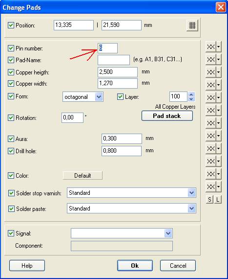
Result:
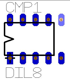
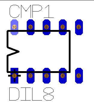
Do the same with the remaining pads of the upper row so that they look that way at the end:
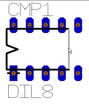
6: now we have to shift the outline of the package. We touch and hold M1H and drag it to shape. You also can hold it and use the arrow keys of the keyboard in order to jump by grid.
and
Confirm the warning message
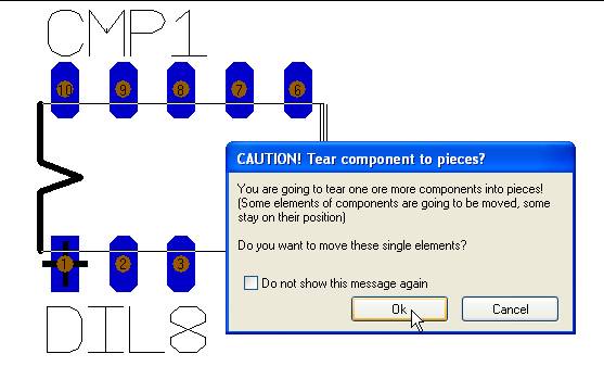
("Yes, you really want to tear it to pieces...")
and get:
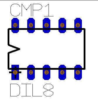
7. Double click the handle cross (at pad N° 1) and change the value from DIL8
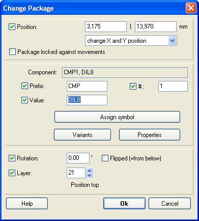
to Dil10. What you get is:
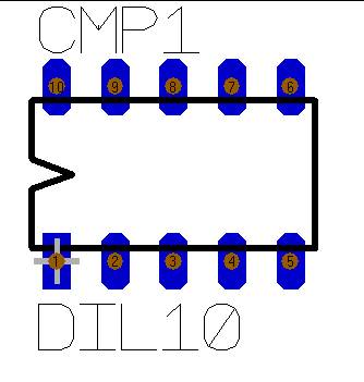
8. Highlight the new package (drawings, solder pads and names must be marked completely) with the mouse.
9. Place the cursor on the spot, where the handle-cross should appear. Attention: It is not necessary to delete the old handle, because TARGET overwrites it automatically.
10. Press the [x] key.
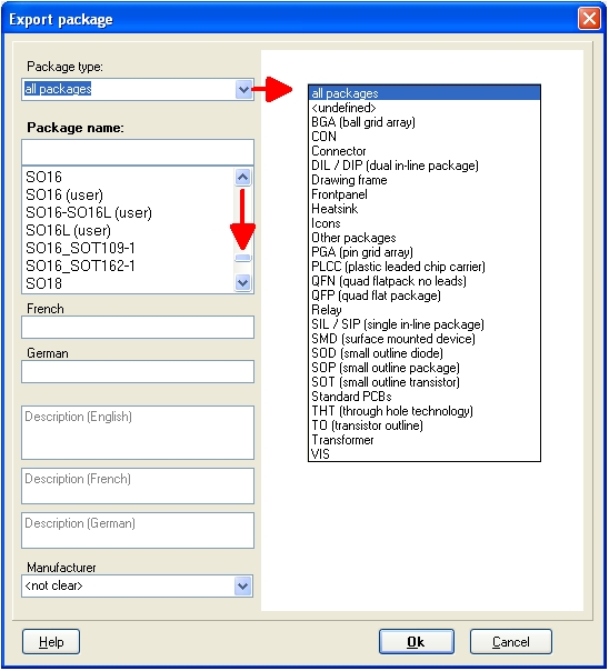
11. The "Export Package" dialog appears. Give it a name and a component type within a component group. For versions older than V14 you would select a library to put it in.
12. Select OK (Return key). Done.
If you intend to assign a symbol to it, please use button "Assign a symbol" in the step 7 dialog.
How to modify an existing symbol
TARGET 3001! allows to modify existing components and export them back to the data base as new components.
Example: You want to change the existing schematic symbol for the smd inductivity SM-B5 into a magnetic shielded smd inductivity SMs35.

1. Open a new project with an empty schematic page.
2. Press function key "F2" and search for component "SM-B5". Now press the "Edit symbol" button. You get asked to create a user copy of it. Confirm this dialog and get the part to the schematic page.
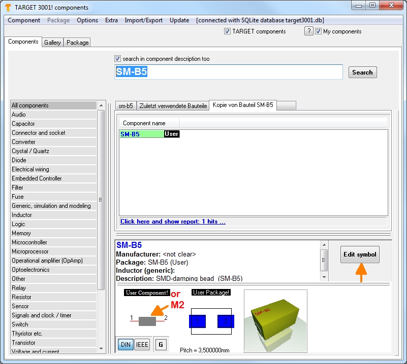
Image: The F2- browser allows edition of a symbol. You also might klick right (M2) on the image of the symbol, bottom left in the dialog.
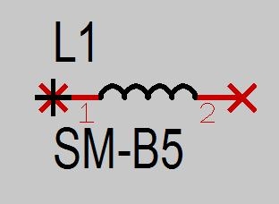
3. For better editing, please select the format filling scale factor with the [F7] key.
4. Now do all the necessary changes with the help of the drawing functions. Take care to have this switch constellation in the sidebar: ![]()
You can of course add new pins, add text or do whichever changes needed.
If you want to delete an element, place the cursor in pointer mode upon an element, press [s] for "select" as often until the element in question is flashing. Now press [Del]. M11 upon the element in most cases does the same.
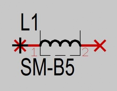
5. Highlight the new symbol (drawings, pins and names must be marked completely!), by dragging M1H in "pointer-mode" a highlighting square over the component.
6. Place the cursor on the spot where the handle should appear (it is recommended to place the cursor on the former location of the handle). Attention: It is not necessary to delete the old handle, because TARGET overwrites it automatically.
7. Press the [y] key for placing the handle.
8. Press the [x] key to export the component.
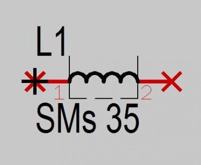
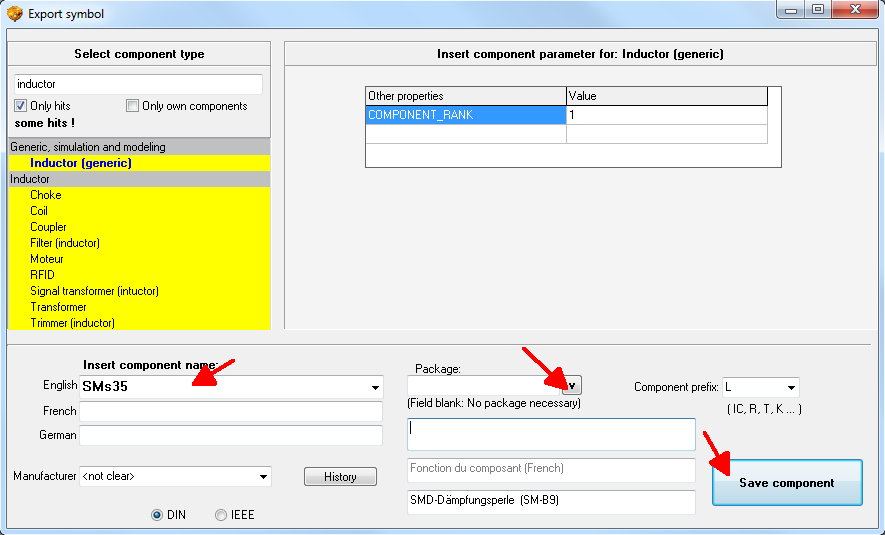
9. Enter all necessary information in the "Export Symbol" dialog.
It is important to choose the right package proposal for your component in the center bottom of the dialog.
Note also: Labelling of an existing component with !COMPONENT, !VALUE or !SYMBOL is not necessary, the existing names can be omitted. Changes and a new labelling are of course possible.
How to draw a package
Before you start drawing yourself, consider whether the package type couldn't be created using the Package Generator. The advantage is that autamatically a 3D model is provided.
You can easily create packages yourself. Say the LTC1392 IC from Linear Technology would not be part of the database. To create this component use the components original datasheet. It can be obtained from the Linear Technologies homepage at http://cds.linear.com/docs/en/datasheet/1392f.pdf
Package outline
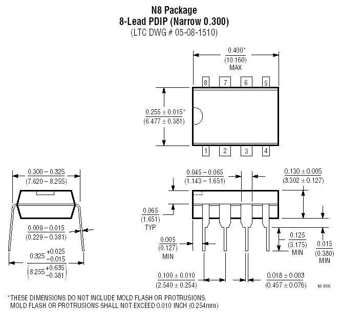
Sketch of a DIP package according to the datasheet measurements of the package, dimension in inches (millimeters):
Sketch of an SO package according to the datasheet measurements of the package, dimension in inches (millimeters):
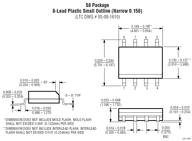
Lets start with the N8DIP package. For a convenient work with this article it might be good to have these two above images printed on paper besides you.
1. Open a new project "PCB with schematic" and switch to the empty PCB page ![]() and select menu View/Toolbars/Toolbar "Edit component" visible to get the toolbar to the left.
and select menu View/Toolbars/Toolbar "Edit component" visible to get the toolbar to the left.
2. Select a suitable grid size. The pitch (= the distance between the centre of two adjacent pins) is 2.54 mm a grid of 0,635 mm (a quarter of the pitch) would be suitable. It is 1/40 of an inch. TARGET 3001! separates decimals by a comma, not a period. Set the above grid unit here: ![]() and here:
and here: ![]() Use the same dialog in order to display only every second grid mark. See dialog:
Use the same dialog in order to display only every second grid mark. See dialog:
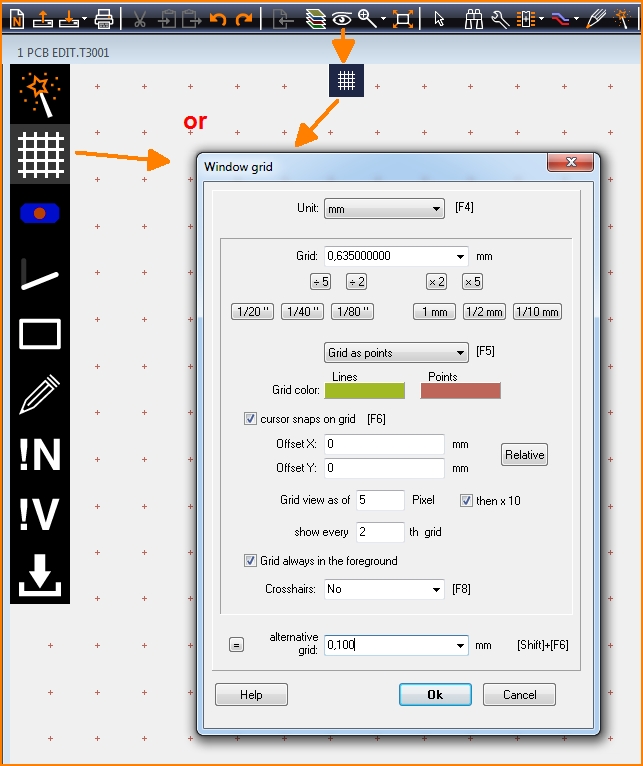
For the package outline a grid of 0,1mm is suitable. That means we have inch-sizes in mind but we set the scale metric, in millimeters (mm).
3. Draw the component outline on layer 21. Clicking the right mouse key on the layer number 21 activates this layer for drawing.

Layer number 21 underlain in gray indicates it being currently ready for drawing on.
After you have chosen the drawing tool ![]() the leftmost layer icon within the main toolbar (top egde of screen) indicates that drawing layer 21 is currently active.
the leftmost layer icon within the main toolbar (top egde of screen) indicates that drawing layer 21 is currently active.

4. Start by drawing an outline of the package. This is done with an "Open rectangle" from the drawing functions. Here the word "open" means "not filled", the opposite of "solid". Use icons ![]() and
and ![]()
Place a rectangle of approximately the same measurement as the package over the origin of the drawing. The exact coordinates of each line of this rectangle will now be entered.
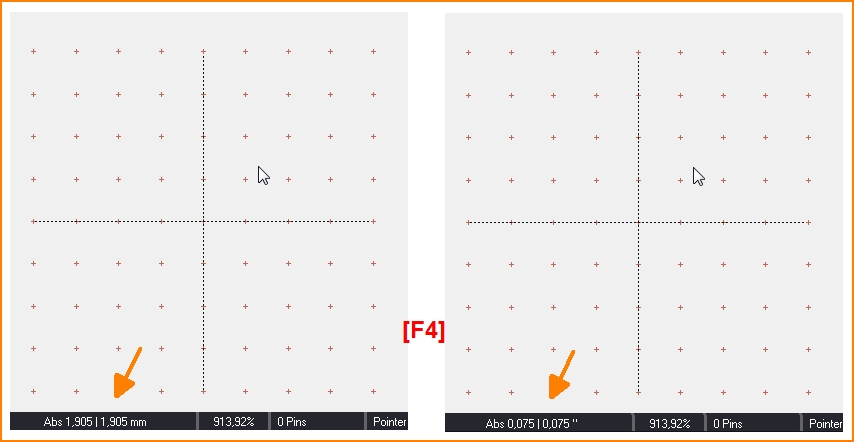
You need to decide if you want to use inch (inch, ") or metric (mm) dimensions. We recommend metric scale in mm. Set the scale in the grid dialog. At any time you can switch the units using the function key [F4]. Set the dimensions of the rectangle within the tolerances according to the value table. For the body we recommend to take the larger values to be on the safe side when assembling the board later. The pitch we set exact without tolerances.
The coordinates in the status bar show the position of your cursor. Keyboard functional key [F4] toggles the units. The image below shows the cursor position in inch at 0,03937|0,06299 ". [F4] toggles to 0,533400|0,546100 mm.
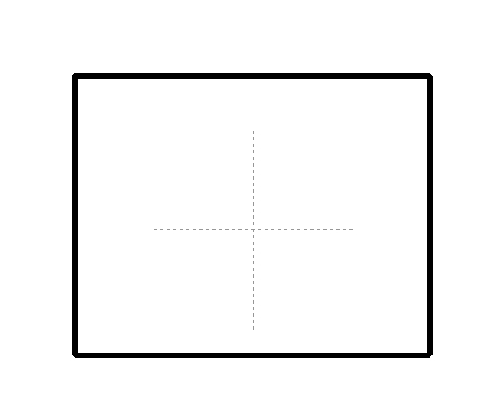
The package shall be constructed, centered around the point of origin. So we start drawing a rectangle of any shape to any place:
"How to get my square to size quickest?"
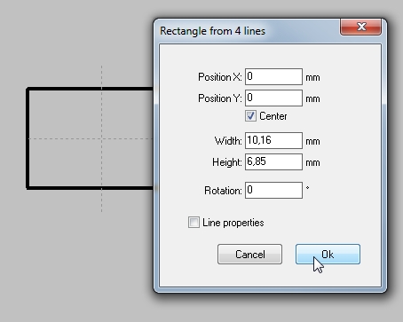
We can see from the datasheet that the width of the package is 10,16 mm and the height is 6,85 mm. Double click a line of the rectangle in order to open a dialog for edition. Set "Position X" and "Position Y" to 0|0 and tick the box Center. Now just enter the measurements for Width and Height and say OK.
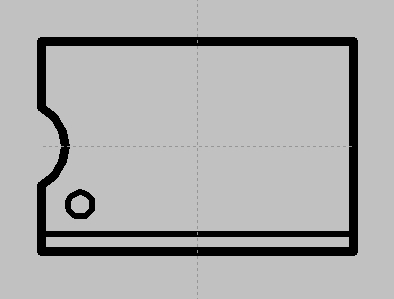
5. An outline of the package with the exact measurements has now been constructed, centred about the point of origin of the drawing. Now, in order to place a notch (mark) on the left vertical line, we select the left vertical line. This will cause little "catchboxes" to appear at the ends of the line and in the middle. Now press M2 upon the middle box and add two vertices. Vertex means another "bending point", represented by another black catchboxes created within the line. Again press M2' at the middle segment and convert it to an arc. Now set a little notch. Also a little circular mark can be set to indicate where Pad 1 shall be placed later. Or a line can be drawn or whatever...
Pads
Wired
6. The next step is to place the pads. The N8 PDIP package has solder pads with plated through holes (PTH) and a copper ring on both copper layers; which is the way a standard pad would appear without the FR4 substrate:

Now select the "place pad" option in the drawing tool:
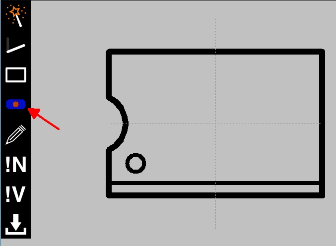
The shape of the cursor will now change to: ![]()
Press the [o] key for options to set the dimensions of the pads being imported. Import them rotated by 90° if wider than high.
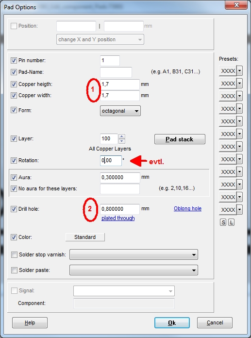
The settings for pad height and width as well as for the drillhole are defined by the datasheet, as shown at item (1) and (2) below.
Pads for wired packages are defined on layer 100, "All copper layers", because the galvanized drilling runs through all copper layers. If you choose a pad default from the selection of the drawing tool ![]() those settings are predefined.
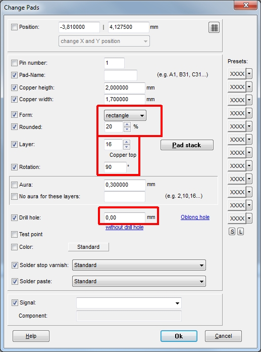
Pads for SMD packages are to be modified in the above dialog a bit: Layer = 16 ("Copper top"), Drill hole = 0mm, Form = rectangle.
those settings are predefined.
Pads for SMD packages are to be modified in the above dialog a bit: Layer = 16 ("Copper top"), Drill hole = 0mm, Form = rectangle.
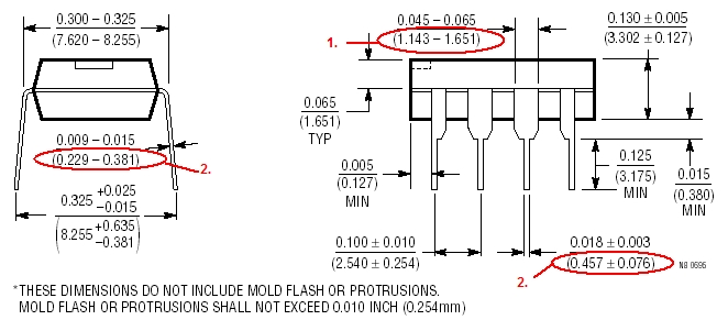
Let us now examine the lead dimensions to define pad dimensions as well as the drillhole diameter. We enter 0,8mm as drillhole diameter (compare at 2, maximum value is 0,533mm so with 0,8mm we're OK). Pad height and width we enter 1,7mm for each (compare at 1, maximum value is 1,651mm so with 1,7mm we're OK).
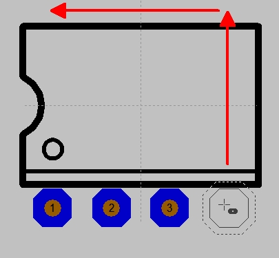
The next step is to place the soldering pads. Set the grid to a quarter of the pitch (2,54mm : 4 = 0,635mm), click the pad icon to the left and start from the center of the body's base line.
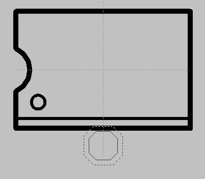
Use the arrow keys of your keyboard and go 6 steps to the left to start with Pad number one. Place it by using keyboard key [1]. Go 4 steps right and press key [1] again in order to place pad number two and so on.
Still use the arrow keys for continuing with the upper row.
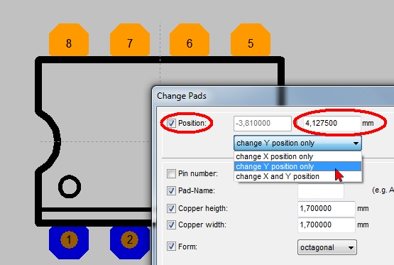
To set the y-coordinate, please highlight the complete lower row and press key [e] for edit. In the flashing dialog change only the y-coordinate to 8,255/2 = 4,1275mm, negative. Do the same with the upper row but change only the y-value to 4,1275 positive.
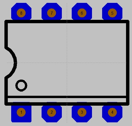
Doubleclick pad # 1 and give it a square form with a corner radius for identification when populating/soldering:
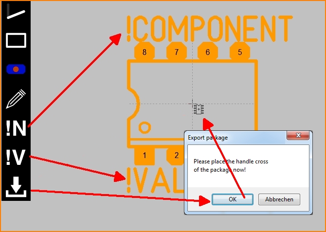
Place a variable component name (will be filled in by the symbol which uses this package) and a variable component value before you click the save icon. Now hover the mouse to the origin in order to place the handle cross there and click. Now you can save the package using an appropriate name.
SMD
For the creation of pads for a SMD package please act similarly. Only the options of the soldering pads have to be adjusted differently:
- The shape of the pads is rectangular with slightly rounded corners (rounded 20% is well. It means: The rounding radius is 20% the length of the shorter side of the pad)
- The drill hole has to be zero (= 0) because there is no drilling
- The copper layer has to be set from 100 to 16 (copper top) or 2 (copper bottom)
The pad dimensions (the landmarks) we draw according to the data sheet. Those are always a bit bigger than the pure leads of the housing.
We from TARGET 3001! draw the pads of an SMD device by default on layer 16 (copper top). So we have defined the mounting of our SMD package upon the copper top layer (the assembling layer). In case you wish to assemble the smd-component on the copper bottom layer (the soldering layer), please use the function "mirror" in the layout later. By this means it is flipped from the copper top layer to the copper bottom layer. Shall a SMD device be assembled on the bottom layer in general so please assign the soldering pads to layer 2 (copper bottom) in the following dialog. For the outline of the package use layer 7 (position bottom). Such an SMD component meant for bottom assembly can be flipped to the upper side later also by mirroring it. When drawing the component please have a cereful look at the drawing view-logic according to the data sheet. Many data sheets show SMD packages in "bottom view".
Question:
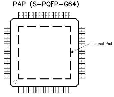
"I am designing a two layer board with Texas Instruments TAS5704 chip (S-PQFP-G64 package) which requires thermal pad connected with vias:
Is there a way to design the package for this chip so that thermal pad is automatically generated?"
Answer:
First draw a normal SMD package as shown above.
The center thermal exposure area create in the same way as a single SMD pad:
- use one SMD pad in square shape like determined by the datasheet
- place as much vias as you need in the inner area by using the full stop key [.]
- move them into position
- connect them to the plane by using tracks (= you must connect them by copper track, only the copper pad is not enough)
- now save the package to the database as usual
- Later when you have imported the package to the layout,
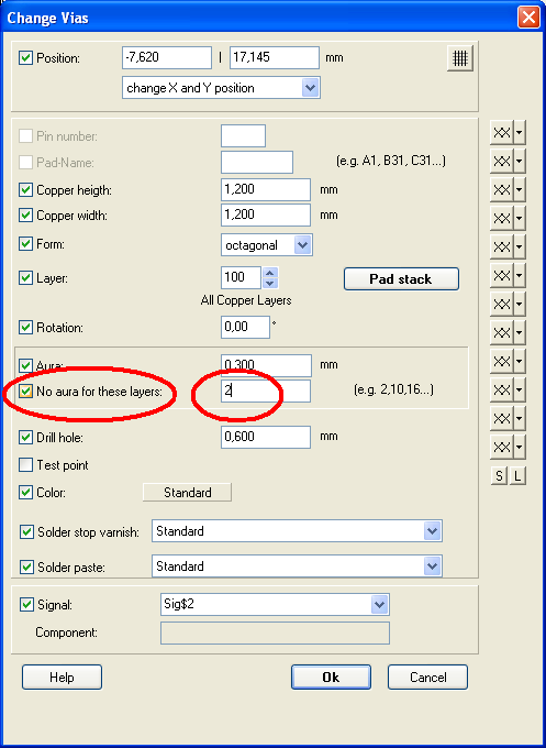
- highlight the inner pads/vias and double click them to open the "Change Vias" dialog:
- use the function "No aura for these layers"
- define the layer on which the aura shall be 0. (maybe 2=copper bottom, maybe 16=copper top)
- set the aura of the tracks to zero (= connect the tracks to the plane)
- give a signal name to the tracks, to the vias and to the plane (as long as this step is not yet managed by the schematic connection)
Save Package
After you have completed construction of the component package, catch it completely (drawing, solder pads and texts) with the mouse M1H.
Place the cursor on the spot where the handle cross should appear (on solder pad # 1 for example).
Press the [x] key (collecting the package with [y] as shown in the schematic is not necessary).
The "Export Package" dialog now appears.
Select the appropriate package type or create one by typing a new one to the line.
Enter a name for the package.
If a manufacturer is known, please select from the list or type in a new one. Otherwise leave it "not clear".
Click OK and the part vanishes from the canvas to the database.
The "Change package" dialog
The "Change package" dialog opens
- on double click upon the handle cross of a package
- on single click upon the handle cross of a package and pressing the keyboard key [e] for edit. Tick box for package and press OK.
The "Change package dialog"
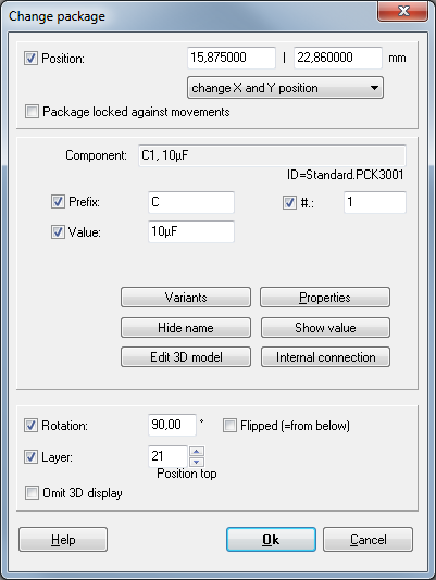
Position defines the coordinates of the handle cross of the package. X- and Y-value can be changed on one strike or only the X-value or only the Y-value, see drop down box. The package will be blocked against any movement if box is ticked.
The line Component contains name and value of the highlighted package. In this line no adjustments can be made. Only in the lines Prefix, Number # and Value. Prefix and number represent the name of a component.
The six buttons mean:
Variants - the maintenance of assembly variants (alternatives of assembly within the same project)
Properties - The list of properties of a component
Hide/Show name - Hide or show the component name (not the package name).
Hide/Show value - Hide or show the component value.
Note regarding earlier versions: Component name and -value can be faded in/out separately in the layout. Fading out by deleting from the layout. Fading in by: Highlighting the package in the layout, hovering the cursor to a place where name/value shall start. Starting the Text mode by pressing the ["] key. In the text dialog selecting Function "Component name" or "Component value".
Edit 3D model - self explanatory
Internal connection - Connections having internal load capacity can be derived from the schematic.
A Rotation of a package by degrees would not be defined within this dialog. Preferably it would be done using [Shift]+[t]. The entry here only shows a rotation which had been effected earlier.
The same with the entry Flipped (= from below) - it is only for announcing whether a part is assembled from the bottom side (box is ticked). No manipulation here - better done in menu: "Edit/Mirror"
The line Layer defines the layer on which the outline image of the package for position print appears. Normally it is layer 21, Position top. But also layer 7, Position bottom, is possible or any other reasonable layer of your choice.
Tick at Omit 3D display effects exactly this: No display of this package in the 3D view of the board.
How to draw a symbol
Easiest would be to use a generic symbol. If there is no match, create a schematic symbol quickest by the use of the Symbol generator:
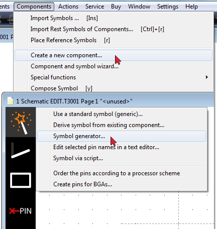
Image: How to open the symbol generator. Prior to the opening of the symbol generator you need to have a component package chosen. If you select "Create_a_new_component#Package_for_layout_use" in Menu Components, please follow the steps to get a package (=footprint pattern) first .
Only if none of the assistant routines will lead to success, you might consider to draw the symbol by hand. But this is easy as well: Use the drawing functions in the sidebar to the left to proceed step by step: Draw the outline, arrange the pins, assign a function to each of them by clicking a pin double. Give the symbol a name and a value, highlight all, hover the mouse to the spot where the handle cross shall appear, press [X] and save it to the database. In the intermediate dialog you assign a package to it and save all. DONE.
To draw it by hand, please use the following routine:
Draw a simple schematic symbol
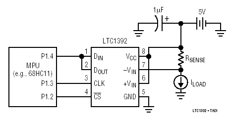
Say the LTC1392 IC from Linear Technology would not be available in the database. To create a component symbol for this IC we have a look at the original datasheet (to be obtained from the Linear Technologies homepage at http://www.linear.com).
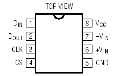
The LTC1392 IC is shown here, top view, set up in a typical application:
1. Open a new project with an empty schematic page by clicking File/New Project on the menu bar
and choose: "Double sided PCB with schematic". You will reach an empty schematic page.
2. Either, use the lines [Ctrl]+[2] or an open rectangle [Ctrl]+[4] to draw the component's outline.

3. Press the [1] key to get the "Place Free Pins" dialog to appear, click OK This will result in the schematic symbol of an IC pin being placed on the drawing. It will be automatically assigned a pin number and pin name as shown below.
Repeat the process until the total number of pins for the particular IC are created and placed one beneath the other on a free area in the schematic.

4. The correct function and proper name of each pin, according to the information given in the datasheet, must now be indicated. To do this, doubleclick M11 on the red pin number section of the pin # 1 symbol. The dialog "Change Pins" will now appear.
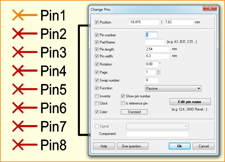
5. Click on the Function drop-down list box and select the pin function of pin #1, which in this case is Input(IN). Further, the pin names shown as Pin1, Pin2 etc, must now be edited to indicate the actual description of the individual pin. This is done by clicking on the "Edit pin name" button to access the "Change Pin Name" dialog box. You can also edit the function "Inverter" and "Clock" (e.g. pin #3) in this dialog. The description of the individual pins can be edited by clicking on the.
6. Select [OK] (Return key).
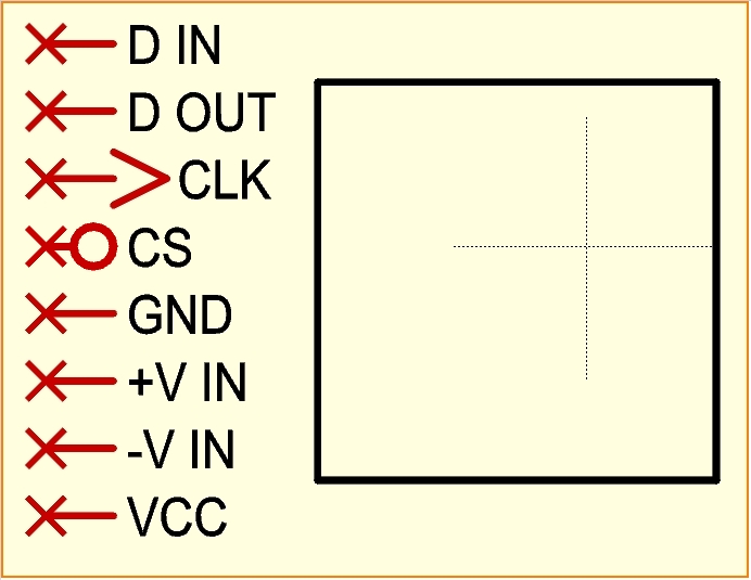
7. Mark all pins with M1 and move them with M1H to the correct location at the symbol. If they need to be rotated around cursor position press [t] for rotation or use M2 for rotation during the displacement.
8. Assign a name and a value each with the ["] key. Select "Component name" in the field: "Function" of the "Text Options" dialog.
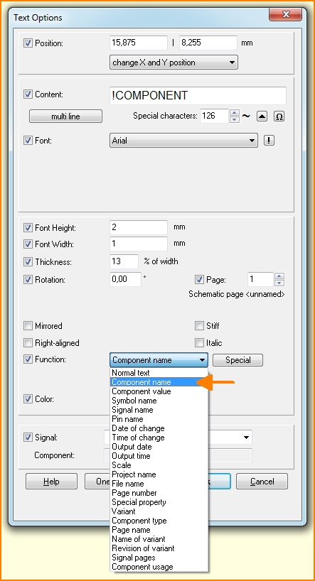
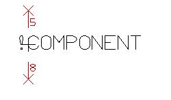
"!COMPONENT" appears automatically representing the components name. Later, this variable will be substituted by the components real designator: for example IC8. Now press [OK]. Place the cursor to another position and again press ["] for opening the "Text Options"- dialog. Please set the text function to "Component value" in the next text option dialog. "!VALUE" appears now automatically as a variable representing the components value. Again, this variable will later be substituted by the components real value, for example LTC1392.

9. Mark (catch) the symbol (rectangle, pins and names must be selected completely!). Do this by dragging a catch window (a highlighting square) by M1H in "pointer-mode". Please Note: The power-supply connections (Pin #8 = VCC and Pin #5 = GND) will be drawn and defined separately, so please leave them aside at first and don't highlight them now!
10. Place the cursor on the spot where the handle should appear (for example in the middle of the symbol).
11. Press the [y] key. All highlighted elements will be assembled now to allow an export to the database.
12. Creation of the power-supply connections:
Please place the connections as shown in the following picture and assign a component name. The pin names can be deleted with the [Delete] key, but they will still exist logically.

13. Highlight the power-supply connection (name and pins must be selected completely) with M1H in "pointer-mode" by drawing a catch window over the symbol.
14. Place the cursor at the spot where the handle of those two pins should appear (for example in the middle of the power-supply symbol).
15. Press the [y] key for placing a handle cross:
16. Click with M11 on the handle and edit the "Change Symbols" dialog:

Symbol No: enter 2 (this means that the component consists of two symbols, a body for the locic functions and a rest for the power supply)
Suffix: enter p for power (power-supply connection)
Insert: choose "Extra Insert as Rest" (power-supply connections will be placed separately as a "Rest of a component" in the schematic)
Why separating the power symbols?
17. Now highlight both symbols by dragging a catch window over all. Press the [x] key to export the component. The dialog "Export symbol" appears:
18. Select the according component group or type in the database, enter a component name, for example LTC1392, press "Save component".
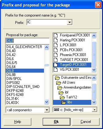
19. Enter "IC" as a prefix.
Select the according package (for example DIL8).
In case you don't want to assign a package to a component (in the case of a reference symbol or a schematic outline frame), you can select <No Package>.
20. Select OK
A symbol with multiple gates
For versions V18 and younger:
In schematic view select item: Components/Create a new component.... The following dialog appears:
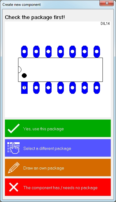
Image: The dialog "Create new component"
A DIL 14 package is suggested - we accept it because for this example we want to create a multiple gate component with four sub-symbols: Three gates of each four pins and a rest of 2 power pins providing alimentation.
Click on green: "Yes, use this package"
You can create a multiple gate symbol with the Symbol generator under the magic wand or you even might draw it by hand. And that is what is explained here. For the fact that it is a DIL 14 package, we just place 14 pins to the canvas and arrange them roughly in 3 groups of 4 pins and two separate, which remain separate a first:

Image: 14 pins placed to the canvas
Double-click a pin, the dialog "Change Pins" opens to define its function (e.g. Input). Click buton "Edit pin name " to give this pin a name name (e.g. In1). Confirm both dialogs with OK.
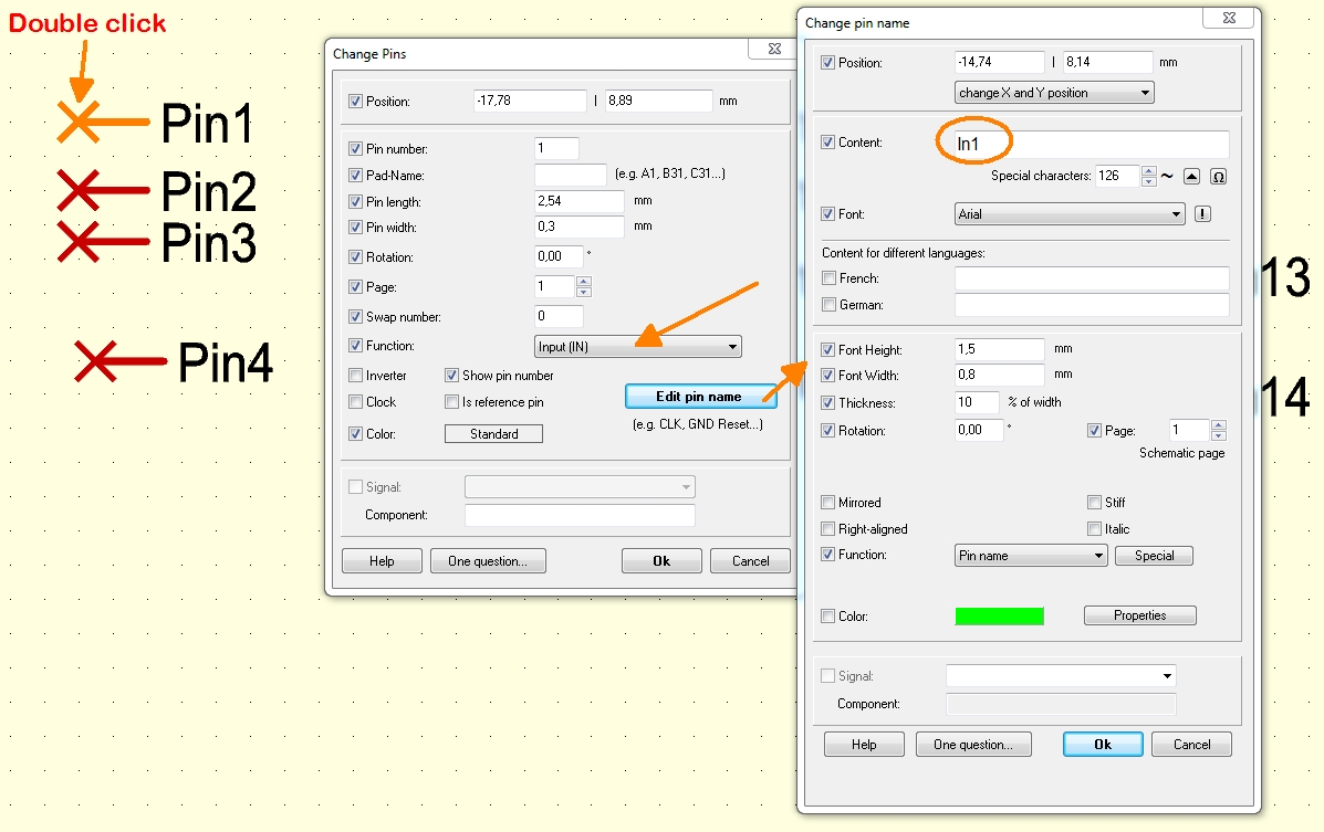
Image: Double click a pin to give it a function (arrow) and a name (arrow).
This is how it looks like for the first pin. Do so for all pins.

Image: Pin 1 function and name given.
Which functions and names you should give is determined by the data sheet of the part. If you are insecure with a function, leave it "Passive". Sure you may give names to your convenience. Proceed like this for each pin and then put them all into neat arrangements of four. Draw a rectangular frame around each set. Place the component name variable ojn top of the box (= button !N at the sidebar to the left) and the value variable underneath it (= button !V at the sidebar to the left).
Highlight such a four-pack including its frame and wording. Now place a handle cross using the button of the sidebar to the left. Proceed as follows for all the three sets of four. If you double-click a handle cross, set each gate to be inserted "automatically as next", which is correct.
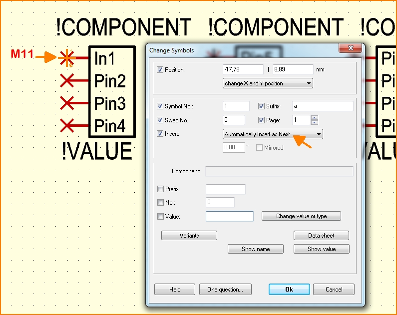
Image: Assignment of the first of the three sub-symbols to be inserted "automatically as next".
The last two pins represent the power connections e.g. VDD and GND. These are kept separate and get inserted extra because they don't play a significant role in the logic of the circuit. Important though, they get inserted as Rest at the end of the circuit design process. Double-click their handle cross. In the flashing dialog set "Insert extra as rest". Now catch all, highlight all and save the entire symbol (i. e. all 4 sub symbols) under a meaningful name.
For Versions V17 and older:
Let's say that the 74ACT11074 from Texas Instruments is not in the component library. To create this component, please use the original datasheet as a reference. This datasheet can be obtained from Texas Instruments homepage under http://focus.ti.com/lit/ds/symlink/74act11074.pdf and contains the following figures:
Top view and logic symbol:
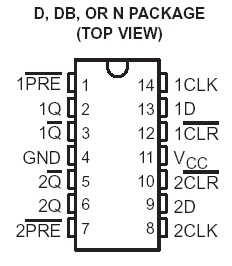
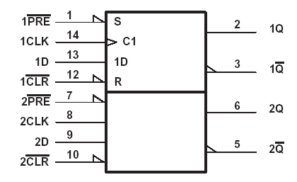
1. Open a new project with an empty schematic page ![]() .
.
2. Draw the symbol with the draw line tool [Ctrl]+[2] or with the draw rectangle tool [Ctrl]+[4]. You should draw all gates at once for a component with multiple gates (for example: 74ACT11074).

3. Place all necessary pins one below each other with the [1] key at a free spot in the schematic. TARGET assigns the pin names automatically.
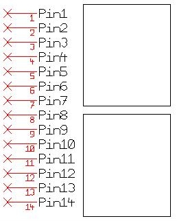
4. Enter the functions of the pin names according the information given in the components datasheet.

5. Click M11 on a pin ( the "Change Pin" dialog appears). Click on "Function" and select the correct pin function (eg Pin #1: Input(IN)). The clock- and/or inverter functions of a pin can be selected here in this dialog (eg Pin #1: 1S\ = Inverter, Pin8: 2CLK = Clock).
6. Change also the pin name here.
7. Highlight each of the pins with M1 separately and move them with M1H to the correct location at the two symbols.
8. Name each symbol using ["] on the keyboard in order to open the "Text Options" dialog:

Enter "!SYMBOL" for the component name and " !VALUE" for the component value in capital letters.
Click on the according function "Symbol name" or "Component value".
Attention: Enter the names only in capital letters (!COMPONENT, !VALUE)
don't enter values like 4K7...

9. Place now a handle cross to each symbol. To do this, please highlight the according symbol (rectangle, pins and names must be selected completely) with M1H in "pointer-mode". Please Note: The power-supply connections (Pin #11 = VCC and Pin # 4 = GND) will be drawn and specified separately, so leave them aside. Do not highlight them now.
10. Place the cursor at the point where the handle should appear (for example in the center of the symbol).
11. Press [y]. Do it for both gates. See the picture.
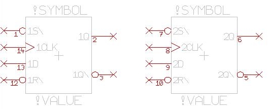
12. Create the power-supply symbol now as described in "Create simple schematic symbol, number 12". Draw it besides the other two gates which you have drawn already. Yur component symbol now consists of three sub-symbols. Now you need to assign the way how it will be imported later:
13. Click M11 on each handle and enter each in the flashing dialog the modifications according to the list:

14. Now highlight the component (two symbols with power-supply symbol) completely with the mouse.
15. Press the [x] key to export the component. The "Export Component" dialog appears. Now save the symbol as described in "Create simple schematic symbol, number 17".
How to draw a reference symbol
Connections over several schematic pages and not visible signal islands of the same signal need to be connected by reference symbols. Please do the following steps to create a reference symbol:
1. Open a new project with an empty schematic page.
2. Draw the reference symbol with the help of the drawing tool ![]() .
.
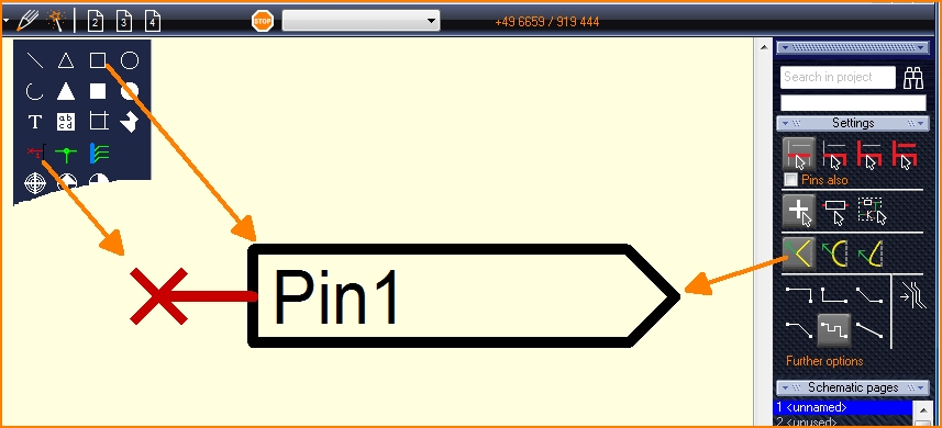
3. Click with M11 on the pin name. (The "Change Texts" dialog appears).
4. Enter the pin name in the first field (text), for example SIGN-OUT. Press OK.
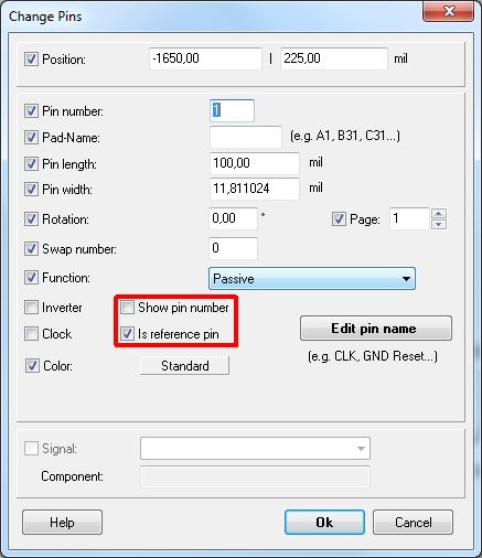
5. Double click the Pin, the "Change Pins" dialog opens. Untick the box "Show pin number" and tick the box "Is reference pin" like in the image below. Then press OK.
6. Highlight the whole reference symbol (drawing, connection) with the mouse.
7. Place the cursor to the spot where the handle shall appear (for example on the cross of the pin).
8. Press the [y] key.

9. Press the [x] key. The "Export symbol" dialog appears.
10. Enter "Reference Symbol to the "Select component type" line.
11. Enter a name for the reference symbol, enter properties if you like and press button "Save component".
How to use the symbol or package wizard
One pad, two or more pins
Where can an exported (edited) component be found?
It plunges into the database and can be found by the name/parameters you had given to it or maybe by the package name. Maybe it is helpful to search only within USER components
(= the range of your components...)
