Difficulties
Symbol and package
Any solderable electronic device has a footprint pattern for the definition of it's solderable pads in the layout. An outline of the housing of the device normally is added. Both in TARGET 3001! are called Package. The electronical logic of a device for the use in a schematic is shown as a Symbol. If you draw a layout without schematic, you only need the package of a device. Symbol and package make a component. Components are stored in the component Component database.
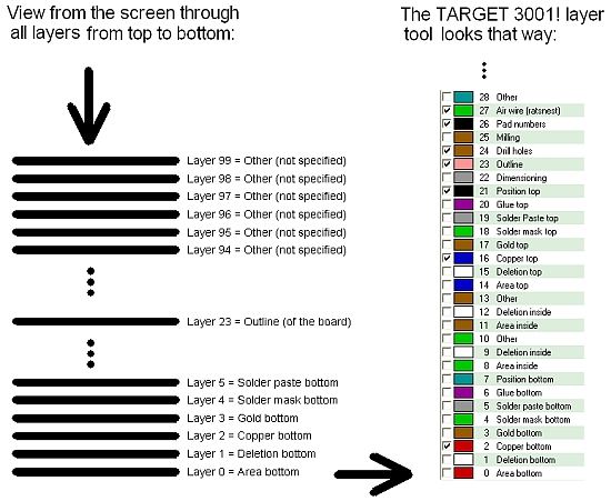
PCB layers concept - why outline layer happens to be 23, etc.
If you have opened the layout view, you are looking through all layers from top to bottom as if they were translucent. This view can not be flipped. The layer tool itself is arranged from bottom to top starting with layer 0 = Area bottom, 2 = Copper bottom and so on.
Any layer can achieve functions different from the default setting, according to your needs.
How to control pad and track sizes
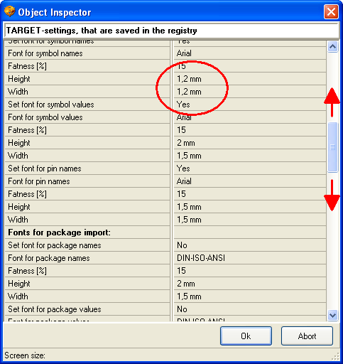
By doubleclick on a certain pad or a certain track and entering to each of the flashing dialogs.For changing the default widths please open the dialog "Object inspector" in menu Settings/Settings Registry...
If you want to change a bundle of elements ex post (after having placed them) please highlight the complete area with a highlighting square and press key [e] for edition. Now you can select one or more kinds of elements (or even all) and adjust them.
The aura of a signal track... Aura what?
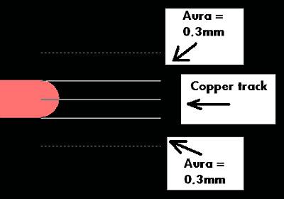
The aura is a security spacing which accompanies a signal track on both sides. Every signal has an aura of 0.3mm by default but it can be adjusted at any time by a M11 on the signal. It is invisible at first but is displayed upon the deletion layer assigned to the respective copper layer. It can be faded in.
With an aura of 0.3mm TARGET 3001! expects a minimum spacing between two tracks of 0.6mm+. If the aurae of two different signals touch each other, a spacing violation is alerted (as far as "Realtime design rule check" in "Menu Actions" is activated). When checking the project electrically later you will get a "spacing violation" error.
Another important function of the aura of a signal is it's isolation function when leading it through a groundplane. All GND-tracks have the aura=0 thus are connected to the groundplane. All non GND-signals need the aura as an isolation spacing to the groundplane.
What to expect as output
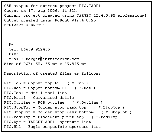
TARGET 3001! offers a huge amount of different output data, see menu File/Input/Output formats. The option "Production" eg offers "(X)-Gerber and drill output PCBout..." If you would use it with our example project PIC.T3001, you would receive the following data generated into a directory of your choice:
The PIC.INFO file is a text file which explains in words which kind of data is needed for the whole project. It is intended as info for the pcb-house. For the pic-project it contains:
Those data are suitable for PCB houses asking you for Gerber RS-274-D the same as RS-274-X (extended Gerber).
Why "check project" outputs errors
The Check project function checks your project against parameters you can set. If at any space a parameter is violated an error message appears. Please see link for further explanations.
Why the project file name becomes "unnamed" in the title bar even if the file name is given
A schematic in TARGET 3001! can have up to 100 pages. Those pages can achieve names. If a page has not a name, it shows "unnamed" in the title bar even if the whole project already has a name. So "unnamed" only refers to the current schematic page.
Airwires
This term means ratsnest. Please see Airwires / Ratsnest.
Why can't I get access to the Component Server?
Maybe you are connected to the internet by a Proxy server? Then please enter Server name, user and Password to the registry. Further info get by the link in the header.
Why the power inputs in the symbols have to be split into parts
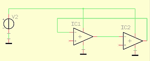
The following circuit uses the principle of a separated power supply which leads to a more clearly arranged logic of the circuit.
The following circuit does not use the principle of a separated power supply. Much wiring is needed for the power supply which might lead to confusion in complex schematics.
When drawing your own components you have the opportunity to draw the power supplies the way that you can import them separately to your schematic later "as rest/remainder", when all the logic work is done. Also busses and reference symbols generally can be used to minimize the wiring.
Why the text is mirrored on the copper side and not on other layers
This is because you see from the top through all layers down to "Copper bottom". Texts written on copper bottom come out mirrored on screen because in reality you have to flip the board to watch the bottom side. You don't have to do so in TARGET 3001!. So texts will be readable "normal" on your bottom side of the board though in the layout you see them mirrored.
Simulation: I have downloaded the BDX53C component from the server. It hasn't got a pSpice Model. How do I add one?
Please see article: Simulation
