Groundplane: Difference between revisions
| Line 116: | Line 116: | ||
You might want to establish another area within your existing groundplane area having has a different potential. First delete your existing ground signal by taking away its signal name. Double-click the ground plane and delete the signal name from the dialog. Now draw the desired shape on the deletion layer. To do this, select the drawing function, hover the mouse to the sidebar to the right and do a click with the right mouse key on the desired layer: ''1'' for deletion bottom or '''15''' for deletion top. Now a deletion layer is activated and you can draw your shape here.<br><br> | You might want to establish another area within your existing groundplane area having has a different potential. First delete your existing ground signal by taking away its signal name. Double-click the ground plane and delete the signal name from the dialog. Now draw the desired shape on the deletion layer. To do this, select the drawing function, hover the mouse to the sidebar to the right and do a click with the right mouse key on the desired layer: '''1''' for deletion bottom or '''15''' for deletion top. Now a deletion layer is activated and you can draw your shape here.<br><br> | ||
| Line 135: | Line 135: | ||
<br><br><br> | <br><br><br> | ||
== Text in Ground plane == | == Text in Ground plane == | ||
Revision as of 13:15, 22 May 2017
I have got a question at this point...
Further links:
How to create a common groundplane by the use of the Groundplane assistant
How to create a freehand groundplane
How to create several freehand groundplanes on one layer
How to create a gridded groundplane
How to remove groundplane islands
How to create a Spacing between GND copper and edge of the board
General
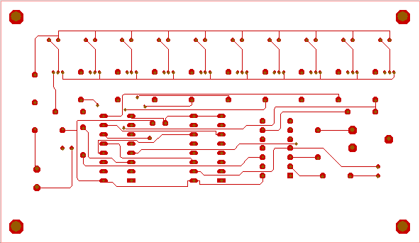
Image 1: A layout without groundplane
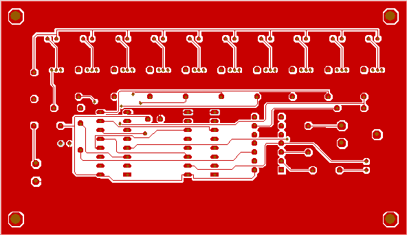
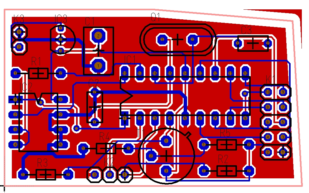
Image 2: The same layout with groundplane (red)
While working with high frequency signals, it is often required to shield them with ground wires or to embed them in ground planes. Using the TARGET 3001! groundplane assistant a groundplane can be generated in realtime on button click. You may generate them solid or gridded. Groundplane islands can be rubbed out.
Groundplane construction in TARGET 3001!
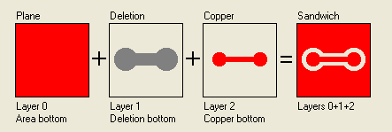
A groundplane in TARGET 3001! is constructed out of three layers:
- The shape of the groundplane (any shape is possible) is defined upon an "area" layer
- The spacings (auras) protecting non-GND-leading signals are defined on a "deletion" layer
- the "copper" layer upon which the groundplane at the end shall appear
Signal tracks not leading the GND signal get separated from the GND plane by a spacing which in the TARGET 3001! nomenclatura is called the aura of a signal. Signal tracks which lead the GND signal get embedded into the groundplane for the very most part.
The area and the deletion layer each must be assigned to the desired copper layer. E.g. if the groundplane shall appear upon layer 2=copper bottom, the area and the deletion layer each must be assigned to this layer 2. The advantage of the TARGET 3001!-graphical area calculation is that any modifications regarding the groundplane area is immediately visible on screen without any time loss.
Tracks leading a groundplane signal should always be routed...
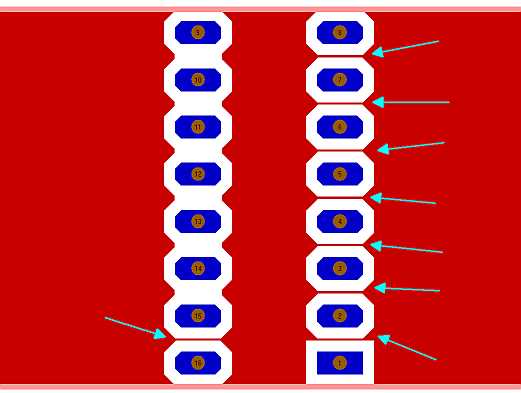
... prior to the generation of the groundplane. Otherwise it is unsure whether a real connection is done or whether it is wide enough. This advice is given though from TARGET 3001! version V15 the groundplane itself effects internal connection from pad to pad (the airwires don't remain). In earlier versions the principle was: "You must rout the airwires by signal tracks." Keep this principle in V15 though because it might happen that the ground signal is not carried throughout all areas of your groundplane because of missing or too narrow copper corridors. The following images will illustrate it.
So in this simple case an interception of the groundplane is obvious. Such interceptions can meander through complex designs and are difficult to figure out at the end. Up to version 14 TARGET 3001! demands that the groundplane signals (GND or any other signal of a groundplane potential), always need to be contacted by routing although those signals might be completely embedded into the groundplane and thus come out invisible. V15 gives more freedom to the user in this point but nevertheless we recommend to always rout ground signals:
In case you can not fulfill the "minimum spacing" requirements, you maybe need to relocate components. Only by this acting all groundplane connections can safely be created. Besides - those little ligaments within the GND soldering pads crossing the pad aura are created by the function Thermal Pads.
Unfortunately it is difficult to figure out whether a connection to ground really is created by a polygon in a sufficient way:
On the left you see only a narrow ligament - sure a reason for an error message. On the right hand side you see more of those ligaments. Now the question is: putting out an alert or assume sufficient? In TARGET 3001! currently you don't need to route the complete GND signal but you should do so. That is to make sure that copper corridors between all sections of your ground plane will have a sufficient width.
Alternatively you will need to visually inspect your groundplane properly wheter all sections have sufficient signal access.
Groundplanes on PCBs not rectangular
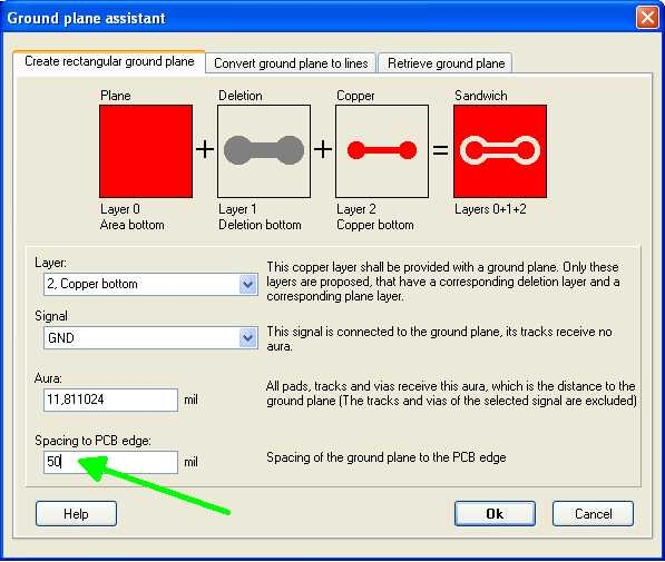
Let's say you have imported a board outline by DXF and now wish to create a matching groundplane. The groundplane assistant can do only rectangular groundplanes covering the whole figure. This is normally no problem, because exceeding parts of the rectangle later it get milled away. You can advise the groundplane assistant to stay back from the edge a certain distance:
This is the result:
The "stay back" line is a copy of your outline double the width of your "stay back" command created on the deletion layer. You can overdraw the exceeding parts by filled geometrical figures on this deletion layer too. But this is only for beauty reasons. For copper top it is layer "15, Deletion top", for copper bottom it is layer "1, Deletion bottom". The same with inner layers.
But sure you can create any groundplane shape you like. Copy your DXF imported outline (which you should have on layer "23, Outline") to layer "0, Area bottom" for a groundplane on copper bottom or to layer "14, Area top" for a groundplane on copper top. Now fill it with matching geometrical figures (there is no "copper pour" on one click). Now highlight the complete groundplane (maybe you can fade out all other layers), press keyboard key [E] for opening the edition dialog, select the desired kinds of figures and assign the GND signal to all of them on one strike.
Please have a look here how to create a custom groundplane: Freehand groundplane
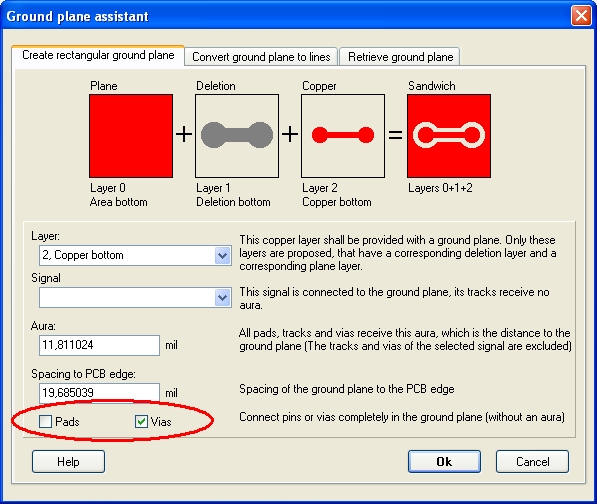
In general a groundplane is connected by the aura=0 of the GND signal. Soldering pads normally keep their aura to prevent the heat from vanishing into the GND area too quick which might cause non connective soldering (also see Thermal Pads). From version 15 you can decide for a soldering pad or a via leading a ground potential, whether to keep their aura or not. in the last case the pad/the via would be connected (embedded) completely to the groundplane. For this reason tick or untick the boxes in the dialog:
Ground plane partitioning
You might want to establish another area within your existing groundplane area having has a different potential. First delete your existing ground signal by taking away its signal name. Double-click the ground plane and delete the signal name from the dialog. Now draw the desired shape on the deletion layer. To do this, select the drawing function, hover the mouse to the sidebar to the right and do a click with the right mouse key on the desired layer: 1 for deletion bottom or 15 for deletion top. Now a deletion layer is activated and you can draw your shape here.
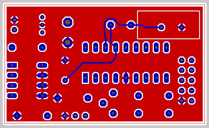
Image: Rectangular deletion top right.
Now choose menu option Actions/Ground planes/Ground plane partition.... The following dialog opens:
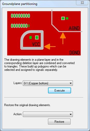
Image: The dialog "Groundplane partitioning".
Select from the dialog whether a partitioning shall take place on the top side or the bottom side: Layers 0 and 1 (copper bottom) or layer 14 and 15 (copper top).
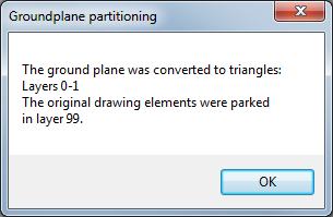
Image: The ground plane partitioning has taken place.
Each area now can be furnished with separate potentials. Click [M1] on the layer and press [e] for edit. Now assign signal names. If you want to have back your genuine area, please find it on layer 99 in order to copy it back to layer 0, area bottom or layer 14, area top.
Text in Ground plane
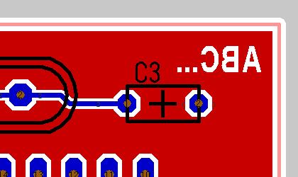
Image: Use the Text function upon layer "Deletion bottom". Mirror the writing by keyboard key [m] in order to make it readable if watched from the bottom side of the board.
Alternatively:
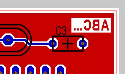
Image: First draw a filled rectangle upon layer 1, "Deletion bottom". Then use the text function upon layer 2, "Copper bottom". Mirror the writing as well so that it can be read from the bottom view. This technique is to prefer against the above version because it doesn't mean too much stress for the ground plane potential (e.g. the signal GND).
Alias: Ground, Erde, Mass, Masse, copper pour
