Track
General
You can reach the draw tracks mode in the layout view...
by [2] or
by "Draw Tracks" in menu "Elements" or
by the tool ![]()
Leave this mode...
with [ESC] or M12
The word "track" in TARGET 3001! is used for a signal track in the layout mode (PCB). A track is the result of the process of routing which means the placement of an electrical connection between soldering pads (footprints). Signal tracks are placed upon the copper layer(s) of a PCB so at the end they come out in copper. Singlesided PCBs have only one copper layer, in most cases "copper bottom". Doublesided PCBs have two copper layers, "copper bottom" and "copper top". Multilayer PCBs have additional inside copper layers.
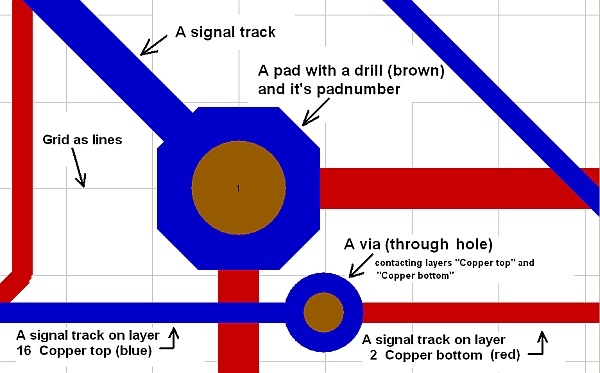
Any element visible might be double clicked for editing (M11).
Establishing a contact
The connections in your PCBs are generated by signal tracks and they behave similarly to signal wires in the schematic part. If you start a track at the end of a ratsnest wire or a defined pad, the corresponding signal name is continued (e.g. GND). If you start from a free pad, the signal name is derived from the pin name (e.g. A1). If you hit nothing special when starting the signal, an artificial signal name is generated starting with Sig$ (e.g. Sig$17). The signal name is shown in the status line at the bottom of your screen.
Snap-on-Pad: If you come close to a pad, TARGET 3001! shows a little Snap-on-Pad box, which attracts the cursor like a magnet. You can avoid this magnetism by pressing [Ctrl] (in reality it is a snap on grid!!) TARGET 3001! generates a beep, if you hit another track or pad. This assures you that the connection really is made.
Please note that the size of a snap on boxe depends on the [[Grid|settings of the grid.] Having set a very small grid, the snap on box gets very small too. So it will be more difficult to hit the snap on box, being crucial for a working connection. Having a grid of 0,01mm this already might lead to the mentioned difficulties. Even if you zoom in very deep into your layout, the snap on box will be rather small.
Backspace Function: To delete the last drawn segments of a signal, you can use the [BACKSPACE] key. This works like "undo" and the start position of the cursor gets adapted too.
Adjust the bending mode while drawing tracks with M2. The [Spacebar] toggles between opposite bending modes, e.g. between both of the 45° bends. An existing track can be edited by displacing of segments [d] or by dragging its corners [g].
If you touch another signal with your new signal wire, TARGET reacts in two ways:
- PCB with schematic: TARGET tells you, that new connections can only be made in the schematic and rejects the attempt placing a new track.
- PCB without schematic: TARGET asks, whether you want to concatenate both signals. If you hit the middle of a signal wire, the wire is automatically split into two segments.
In "Draw Tracks" mode, you can manually place a via, by pressing [.] (full stop). Signal layers are changed, see status line at the bottom of your screen. You can change track layers without generating a via by pressing [:]. Besides: You bring an already imported component to the opposite layer by mirroring it. Highlight it and press key [m].
How to activate a certain routing layer
In the sidebar on the right side of the screen, you can right-click the layer number to activate the copper layer on which the tracks shall be placed. The layer will then be highlighted in copper color and its number and color will immediately appear on the left side of the layer history (= currently active drawing layer). If you check the color box of a certain layer in the sidebar by clicking on it, this layer now will be visible in the layout (faded in). Removing the tick means that this layer will be faded out of the layout (but not deleted!)
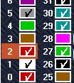
Image: You now will be routing on layer 2, copper bottom.
If you move the cursor close to a solder point, you can place the signal directly with 'M1. TARGET 3001! automatically connects the signal to the corresponding solder pad. A little square at the solder pad helps hitting the signal exactly with a small snap on box. You can circumvent this function by the [Ctrl] key.
Note that the size of the snap box depends on the Grid Setting. With a very small grid, the snap box will also be very small, so that the required "central" connection of traces, i.e. hitting the snap box, will be more difficult. With a pitch of 0.01mm this problem could already occur. Even if you zoom deep into the layout, the snap on box will be very small. If the snap on box does not appear at all, you might be routing on the wrong layer.
Alternatively you can activate the routing layer in the toolbar by clicking one of the routing history fields:

Image: The layer history
Left shows the currently active layer (16), right beside it the recently used layers (2, 13 and 10) which you can click for activation. If there is a 99 inside this means: None used so far. By the "routing history" you cannot "set" a certain layer in order to use it. You can only select already used layers. In addition to clicking with the mouse, there is also a shortcut mechanism, which is explained below.
Change routing layer
In a two-sided layout
If you want to change the copper layer while placing a track, press the keyboard key [.] (full stop). At this point, a via is set and the current track layer is changed. If you were on the copper top layer, TARGET switches to the copper bottom layer and vice versa. You can recognize this by the change of color when routing a track on the other layer. The key [:] changes to the opposite copper side / layer, without setting a via. By the way: You bring a component to the other side of the PCB by mirroring it (mark the component and press [m] key). Mirror axis is cursor position. So don't move away the cursor too far. The part might flip out of screen.
In two- and multilayer layout
Use the layer history:

Image: The layer history: The active drawing layer is displayed on the left side, the previously used layers on the right side.
The [,] (comma) key can be used to quickly switch between layers when drawing tracks. Multiple presses have different functions:
The next layer of the history is selected with the 1st press. A second press (without any other action) selects the next but one layer and so on.
Example, see picture:
Active drawing layer is 16, copper top, indicated by positioning to the left in the layer history. The first press on the comma key changes from level 16 to layer 2, another press selects layer 13, pressed again selects layer 10.
With action between presses: The first press on the comma key changes from layer 16 to layer 2, now place a track. Press again selects layer 16 again.
By the comma shortcut you can quickly switch between layers without creating a via or leaving the mouse position in the layout.
alias: Change component layer
Swap layers: Shift all tracks from copper top (Layer 16) to copper bottom (Layer 2) and vice versa
If you shift a track to any non track layer it loses its track properties and ends as a bare line. From this situation the track properties can not be recovered! So you need a third copper layer as a kind of a "interim parking". The editions discover, light, smart und medium have only two copper layers...
Solution:
Set a free layer e.g. layer 33 to function "Position top". Now shift all copper tracks from 16 to 33. Now all tracks from 2 to 16 and all "Bridges" from 33 to 2. Lines with a signal upon position layers (like silkscreen) are taken as a bridge and keep the signal.
Placing a bridge
You can insert bridges by pressing the [b] key. The actual segment then still is placeded as a track, the next segment gets a bridge. The length of the bridge is defined by clicking M1 at the desired distance.
Track options
Press key [o] for applying options for coming actions. The following dialog opens:
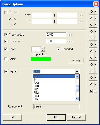
Track width: Please enter the width of the tracks you want to place.
Track aura: The tracks you will place will be added into the according deletion layer. The size of the aura will be added to each of the tracks size in this layer and be used to calculate the distance to ground planes.
Rounded: The ends of a track will get round caps. This causes smart connections of segments with sharp bends.
Layer: means the location (layer) on the board, on which the tracks will be placed. Usually, copper layers are used.
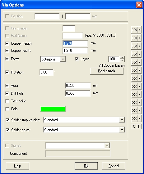
-->Via: Opens the via options dialog:
Save a set of track options with the XX-buttons to the right of the dialog. Use the little arrow right beside for explanations.
Some signal properties are very important for the auto router. They must be set in the schematic signal wires properties dialog:
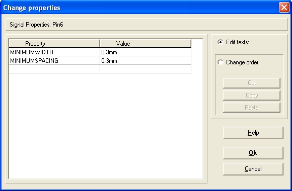
This is the setting of the track width and track spacing in respect to the autorouter's work...
Streamline a track
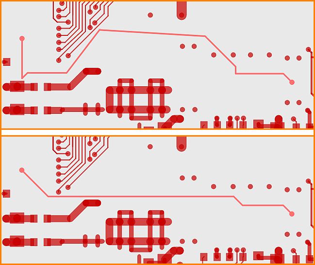
Image: Before-After
With the key [7] (attention: not [F7]) you can tighten a selected conductive track. Collinear pieces are combined, all inclined tracks are brought into a 45° angle grid, tips are cut off, 90° angles are bevelled and unnecessary detours are avoided. It also works when multiple tracks are selected. All obstacles are of course taken into account.
Deleting a track
Highlight it and use the [Del] key from your keyboard.
"But what if I can't touch it because it is covered by another element so that I can't highlight it?"
Solution: Hover the mousepointer to the spot where the desired element is placed. Now press keyboard key [s] as often until the desired element flashes. Press the return key to have it highlighted. Now delete it.
Delete all traces on one slab
Use [Ctrl]+[a] to select the entire layout. Now press [Del]. The removal mechanism works in three steps: the first time you press it, all tracks that have been laid by an Autorouter are deleted. The second press deletes all manually laid tracks. The third press deletes everything else. Too much deleted? Press Undo.
.
