Crash course
The following crash course has been reviewed in March 2012. Download it in PDF-format (567 kb)
You find it too long? Find a quicker one here: CrashCourse2
Introduction
Target 3001! is an object focussed schematic-, simulation-, and PCB CAD-software for PC in English, French and German language. It is a partly automatic tool, supporting you when drawing schematic, running a simulation, and layouting the PCB including an EMC-analysis (electromagnetical compatibility). TARGET manages schematic, simulation, PCB and EMC-check as one so that modifications are implemented simultaneously whithin the other part or are at least considered. Each TARGET project refers to one single database. No error causing conversions of different data formats!! TARGET is a worldwide unique software system combining the above mentioned properties whithin one user interface. TARGET supplies enlargeable component-, model- and package libraries. It is able to create a bill of material and netlists. Components can be placed by hand or automatically. They can be edited at every time and easily be displaced after selection. You can route your PCB on screen interactively or use an autorouter. Your PCB can be transformed into CAM-data with the help of the numerous export drivers.
A free version for discover can be downloaded from www.ibfriedrich.com
Conventions for this Crash Course
[x], [Alt] expressions in square brackets mean "press key" on the keyboard or press a button in a dialog.
![]() pictograms mean icons on the toolbar.
pictograms mean icons on the toolbar.
"Abcd" expressions in quote mean dialogs, menues, menue commands or entries in pull down menues (e.g. name of component in a component library).
Mx Expressions beginning with M are mouseclicks
Dialog: the word "Dialog" in front of an expression means the header of a window or a dialog field
![]() Single arrow means: "press...!", "switch...!", "choose ...!"
Single arrow means: "press...!", "switch...!", "choose ...!"
![]() Double arrow means: it follows ..., it arises...
Double arrow means: it follows ..., it arises...
Example:![]() [o]
[o] ![]() Dialog: Options
Dialog: Options ![]() Track width 0.3 mm
Track width 0.3 mm
Means: Press key [o], the dialog "Options" will open, set track width to 0.3 mm.
Press key [Esc] for returning to the pointer mode. You also might press M12.
After starting TARGET 3001! the start assistant opens. With its help you can open an already existing project or start a new project (with or without PCB). After selection the "schematic mode" is shown. You can see the header, the menue line, the toolbar, the working area (canvas) and the status line. If you just move the cursor over a button without clicking, an info flag is shown describing the function of the tool.
The buttons of the toolbar in the schematic mode
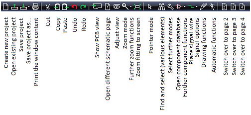
Tools with extensions offer a selection of further functions, sub-functions, options or entries of parameters.
Examples:

![]() M1 on transistor-symbol
M1 on transistor-symbol ![]() the main function import component is activated.
the main function import component is activated.
![]() M1 on
M1 on ![]()
![]() further component import functions e.g. import rests of components or insert reference symbols can be selected.
further component import functions e.g. import rests of components or insert reference symbols can be selected.

![]() M1 on signal button
M1 on signal button ![]() the main function place wire is activated
the main function place wire is activated
![]() M1 on
M1 on ![]()
![]() a menue of signal options opens e.g. bending mode or track width can be selected.
a menue of signal options opens e.g. bending mode or track width can be selected.

![]() M1 on wizard symbol
M1 on wizard symbol ![]() a pull down menue contending automatic functions is opened e.g. start simulation or check project.
a pull down menue contending automatic functions is opened e.g. start simulation or check project.
Mousekeys in normal mode (pointer mode)
Left: M1, M11, M1H... Aselection and edition of all drawing elements
Right: M2 opens a context menue concerning the view of the schematic
Zoom functions:
M22 zoom out (diminish)
M2H and drag right: catch a window and enlarge
M2H and drag left: the entire schematic is shown fit to screen
Middle: M3 zoom in (enlarge the area around the pointer
Left and right simultaneously: M12 current action is cancelled ([Esc]).
Schematic mode
This chapter will show you by an example, how to draw a schematic. The following schematic of a switch-delay by monoflop is to be drawn:
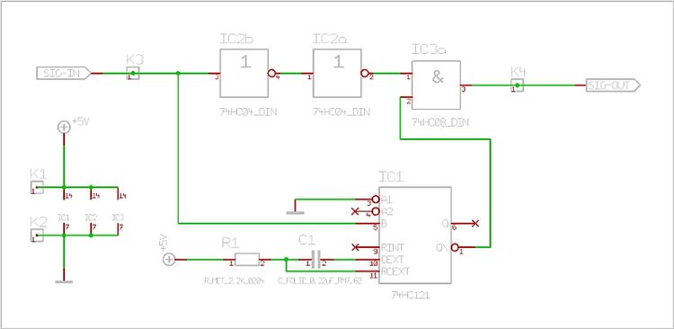
Start a new project titled: s_delay
![]()
![]()
![]() Dialog: Create new TARGET project.
Dialog: Create new TARGET project. ![]() file name: s_delay . TARGET creates the extension .T3001 automatically. In spite of drawing a schematic, you mustn’t activate the switchbox "Create PCB without schematic".
file name: s_delay . TARGET creates the extension .T3001 automatically. In spite of drawing a schematic, you mustn’t activate the switchbox "Create PCB without schematic".
![]() [OK]
[OK] ![]() 1 Schematic s_delay.T3001 Page1 "<unnamed>"
1 Schematic s_delay.T3001 Page1 "<unnamed>"
Maximize the empty schematic fit to screen. The area of the opened schematic page (canvas) has the size of 1,44 m² or 5511.58 in².
For an easy handling of your drawing...
Insert a frame DinA 4
![]()
![]()
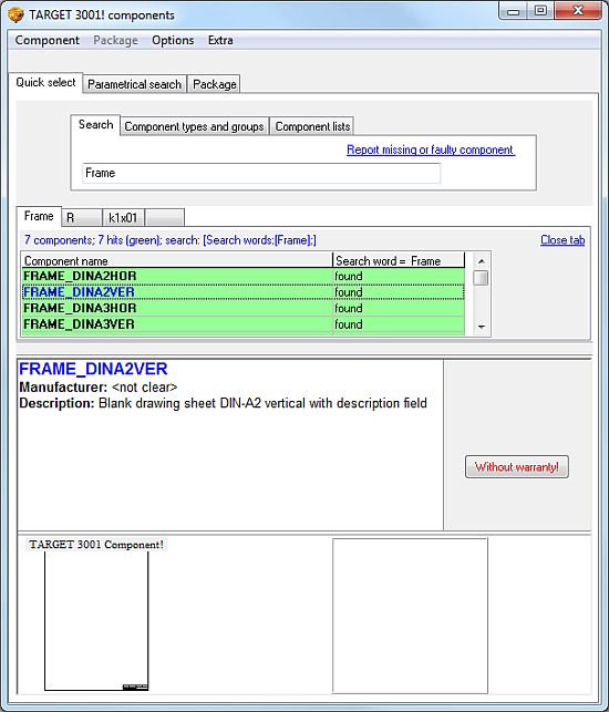
![]() Dialog: "TARGET 3001! components" showing:
Dialog: "TARGET 3001! components" showing:
- The tabs: "Quick select", "Parametrical search", "Package". Below a search field offering search option in various pools.
- The search results (green area)
- A "Name and description" area
- An image zone for symbol, package and 3D view (if applicable)
![]() Frame
Frame ![]() Blank drawing sheet_DINA4VER (from search results list),
Blank drawing sheet_DINA4VER (from search results list), ![]() [Import Component]
[Import Component]
The frame now appears on your screen. It is fixed to the cursor and can be dropped by M1. M12 quits this action. You might also press key [Esc] for getting rid of a component being fixed to the cursor or leaving any mode and returning to the pointer mode. Zooming out by mousewheel makes the entire frame visible on screen.
Before inserting components you should...
Switch on grid
![]()
![]()
![]()
![]()
![]() Dialog: Window grid.
Dialog: Window grid.
The grid spacing should remain 25 mil (=1/40" =25/1000" =0,025" =0,635mm) because most components are based on this grid. Instead of "Grid invisible" select "Grid as points". The other settings on this window remain as preset. Especially
After ![]() [OK] a grid of points is visible if not the scale may be too small. Zoom in by M2. The grid will ease the drawing of signal wires and will help you when...
[OK] a grid of points is visible if not the scale may be too small. Zoom in by M2. The grid will ease the drawing of signal wires and will help you when...
Inserting components
Act like described in section "Insert a frame DinA4"!
NOTE: Shall the matching of your circuit later be simulated please select only components fitted to a simulation-model. Choose in the database dialog: "TARGET 3001! components" the tab "Parametrical search". There you can tick a box to ask for search results oly including a simulation model. In this crash course we abandon the simulation so we may leave this box unticked (the number of matches will be bigger then).
Return to the tab "Quick select". The components 74HC04_DIN, 74HC08_DIN and 74HC121, the resistor R_MET_2,2K_0204, you will directly find in the database. Just type in those strings to the search field.
Regarding the capacitor use: bipolar capacitor; foil; 0,022u and press "Enter" or the "Search"-button. The semicolon separates search words. Sure you also might use te "Parametrical search" in order to find the desired devices.
In respect to the connectors K1....K4 use the quick search simply using "1x1". In the english and french language version connectors have prefix "C" instead of "K".
The connectors K1 ... K4 you will also find named C1X1 (without simulation model). They will only be used for a later creation of a PCB with connectors (e.g. soldering nails, edge socket connectors, receptacles).
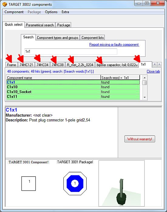
Image: Database dialog. If you want, you can search each part within an individual tab (red arrows).
Consider clever placement of the components so that subsequent placing of the signal tracks can be done with a small number of bendings. During the import of a component you see it be fixed to the cursor like a phantom. M2 causes a 90° rotation of components (counterclockwise). After insertion of the symbols/components please insert the symbols for ground (GND), power supply (VCC) and input and output signal. You will get this by...
Import of reference symbols
![]()
![]() of the button
of the button ![]()
![]() [import reference symbol]
[import reference symbol] ![]() Dialog: TARGET 3001! components.
Dialog: TARGET 3001! components.
The same database dialog opens showing the component type: reference symbols. The symbols required (GND, V+, SIGN-IN and SIGN-OUT) can be imported into your schematic the same way we did with the other symbols.
Import rests of components
Some real components are usually not drawn completely in schematics. Especially when drawing digital elements the power supply is for reasons of an easier overview not drawn. But if you want to manufacture a PCB you have to make sure that the corresponding connectors do exist. TARGET offers power supply symbols as "Rests of components" to be inserted into the schematic and to be connected to the reference-symbols (e.g. +5V and GND):
![]()
![]()
![]() [Import Rests of components]
[Import Rests of components] ![]() Dialog: Import remaining components.
Dialog: Import remaining components. ![]() Select component (ICx,xxxx),
Select component (ICx,xxxx), ![]() ICxp import =as rest (p stands for power)
ICxp import =as rest (p stands for power) ![]() [OK]
[OK]
![]() Place power symbol into schematic.
Place power symbol into schematic.
Displace symbols
Click with M1H on the handle (snapping cross) of the component and displace it with mousekey held (drag & drop). If this action does not work, please adjust the following sidebar icons:
If this button ![]() is activated, you will highlight a component completely only if you hit the handle cross.
is activated, you will highlight a component completely only if you hit the handle cross.
If this button ![]() is activated, you will highlight a component completely even if you hit only a part of it. So if you release this button you can displace single elements of a component (e.g. writings) by M1H. Danger: components now can be torn apart. But a warning appears. For displacement of more than one symbol on one strike, you first have to highlight each of them by [Shift]+[M1] or by opening a marking area (catch window) by M1H.
is activated, you will highlight a component completely even if you hit only a part of it. So if you release this button you can displace single elements of a component (e.g. writings) by M1H. Danger: components now can be torn apart. But a warning appears. For displacement of more than one symbol on one strike, you first have to highlight each of them by [Shift]+[M1] or by opening a marking area (catch window) by M1H.
Entries of component values
Click M11 on the handle of a component ![]() Dialog: Change Symbols
Dialog: Change Symbols
![]() Value: enter any other value (e.g. for C1: 20nF instead of BIPOL)
Value: enter any other value (e.g. for C1: 20nF instead of BIPOL)
Connection of components
TARGET 3001! calls connections "signal tracks" (in short: signals or wires).
![]()
![]() leads you to this mode and the cursor shows as a cross. The hit of a pin by M1 is confirmed by a beep and the cross at the pin fades in order to show the connection. A thread is fixed to the cursor now.
By M2 or using the spacebar the bending mode during the placement of wires can be changed.
TARGET 3001! itself chooses a name for the signal, see status line. If you don’t like this name, change it while placing wires:
leads you to this mode and the cursor shows as a cross. The hit of a pin by M1 is confirmed by a beep and the cross at the pin fades in order to show the connection. A thread is fixed to the cursor now.
By M2 or using the spacebar the bending mode during the placement of wires can be changed.
TARGET 3001! itself chooses a name for the signal, see status line. If you don’t like this name, change it while placing wires: ![]() M11 or
M11 or ![]() [o]
[o] ![]() Dialog: "Signal Wire Options"
Dialog: "Signal Wire Options" ![]() Signal: enter new name.
Place all segments of a signal by M1 and quit every signal with M12 or [Esc]. The latest placed segment can be deleted with [Del].
Signal: enter new name.
Place all segments of a signal by M1 and quit every signal with M12 or [Esc]. The latest placed segment can be deleted with [Del].
TARGET 3001! offers lots of further options and tools for editing signals.
PCB - mode
Now we want to create a PCB from our above drawn schematic. You must now ...
Switch over to PCB-view
Now you get asked to define an outline of your board. You see preset measurements of
Width: 6299,0000 mil
Height: 3937,0000 mil
...it is a result of presetting the metric EURO card format which is 160mm width and 100mm height. Sure you easily can adjust it.
![]() Press button "Complete PCB outline"
Press button "Complete PCB outline" ![]() Dialog: Auto placer
Dialog: Auto placer
You can use the auto placer or cancel it. For this example we cancel it. Now you see an empty PCB on screen.
New buttons are:
![]() to the schematic view (toggle) highlighted component is shown in the schematic
to the schematic view (toggle) highlighted component is shown in the schematic
![]() configure layers
configure layers
![]() import package / else
import package / else
![]() draw track / track options
draw track / track options
![]()
![]()
![]()
![]() select previously used layer for drawing. The left one shows the currently used layer
select previously used layer for drawing. The left one shows the currently used layer
The most important thing is that the sidebar has changed as well.
Show grid
See above.
Advice:
During PCB layout the window grid scale is important. In most cases a grid of 25 mil = 25/1000 inch =0,635 mm is best, because normal spacings of component pins are based on this inch scale. E.g. the spacing of two neighboured IC pins =2,54 mm = 4*0,635 mm =100 mil. Deviate from the preset grid value only for important reasons (e.g. 0,3175 mm, if the track width has to be smaller).
In the grid dialog you should tick the box: "Cursor snaps on grid" or use functional key [F6].
Show cross hair
Use functional key [F8].
Definition of the layers
The elements of a PCB e.g. package, signal tracks, drill holes... each are placed (drawn) upon different layers. All layers are placed over each other. So what you see in the PCB view is a look through all layers from top to bottom. TARGET offers layers 0 to 99. For reasons of saving screen time you should only fade in the layers in need.
![]()
![]()
![]() PCB-layers
PCB-layers
For a usual single sided PCB fade in (tick) layers:
- 2 for copper bottom
- 21 for packing on top
- 23 for drawing the outline of the PCB
- 24 for drill holes
- 26 for soldering pad numbers and
- 27 for air wires
Set the function of layer 16 to "other" (instead of "copper top"). To do so, please use the layer tool and doubleclick the line which shows the layer function. By this means you will avoid placing signal tracks on this layer.
Define the size of the PCB
a) If you haven't done it already you can define the size by
![]() Menu: "Actions/PCB Outline Wizard"
Menu: "Actions/PCB Outline Wizard" ![]() Dialog: PCB Outline Wizard. Follow the dialog to define the outline of your PCB on layer 23.
If the size later isn’t exactly to your wishes, catch the right or the upper half of the PCB with a catching window and move it by M1H. Make sure to release the resistor-symbol
Dialog: PCB Outline Wizard. Follow the dialog to define the outline of your PCB on layer 23.
If the size later isn’t exactly to your wishes, catch the right or the upper half of the PCB with a catching window and move it by M1H. Make sure to release the resistor-symbol ![]() within the sidebar. You can read the measurements directly within the status line (bottom of screen).
within the sidebar. You can read the measurements directly within the status line (bottom of screen).
b) As an alternative you can draw an outline ![]() Drawing functions
Drawing functions ![]() Draw open rectangles on layer 23 of desired size. After having chosen this tool, please hover the cursor to the side bar layer number 23 and do a click M2 upon this number in order to activate this layer for drawing. Now hover the cursor to the canvas and draw.
Draw open rectangles on layer 23 of desired size. After having chosen this tool, please hover the cursor to the side bar layer number 23 and do a click M2 upon this number in order to activate this layer for drawing. Now hover the cursor to the canvas and draw.
The PCB outline appears as a rectangle, coloured the same as the colour of the outline layer, pink by default. If you do not see anything, maybe the layer 23 is not faded in. Do so by ticking the colored box of layer 23 in the sidebar.
Help: Select the complete outline ![]() [e]
[e] ![]() Dialog: "Change Lines". Adjust layer to 23 in case it is different.
Dialog: "Change Lines". Adjust layer to 23 in case it is different.
Define mounting holes
![]() Menu: Elements
Menu: Elements ![]() Place mounting drill hole. Drop them by M1 to an appropriate place on the board. Edit them by following the dialog after M11 on it.
Place mounting drill hole. Drop them by M1 to an appropriate place on the board. Edit them by following the dialog after M11 on it.
Import and placement of component packages
The remaining area offers space for import of the component packages corresponding to the symbols used in schematic.
General remarks: First place those components with a fixed (non variable) position to the PCB (e.g. interfaces at the edge of a PCB ). Then place the biggest ones (those components of central meaning or those with lots of pins). Last but not least place the smaller ones into remaining spaces. As a help for placing, TARGET 3001! shows air wires to the pins of the component most close to when importing or displacing components. This display is computed after every movement and eases a favourable placement of the packages. A crossing of two air wires can often be avoided by rotating one of the packages by M2 at 180°. Place packages carefully and leave enough space for later placement of the signal wires (on the edge of the PCB as well). In other words : The worse you prepare your PCB the worse signal tracks are to be placed and routed without touch.
Now we want to get the corresponding packages out of the libraray:
![]() [Import package] or
[Import package] or
![]() [Ins] or
[Ins] or
![]()
![]()
![]() Dialog: Import package for
Dialog: Import package for
The list at first shows all package proposals. The kind of ranking within this list can be adjusted.
Corresponding to the above mentioned rules first select one of the connectors (K1, ..., K4), e.g.:
![]() K1,K1X1
K1,K1X1 ![]() [OK]
[OK] ![]() select package (vgl. Import component, described as in 1.2)
select package (vgl. Import component, described as in 1.2)
Within the opened library TARGET 3001! has yet highlighted the recommended package 1X01 .
Accept the suggestion by ![]() [OK] and place it by M1 (e.g. in the corner top left beneath the drill hole) on the PCB.
[OK] and place it by M1 (e.g. in the corner top left beneath the drill hole) on the PCB.
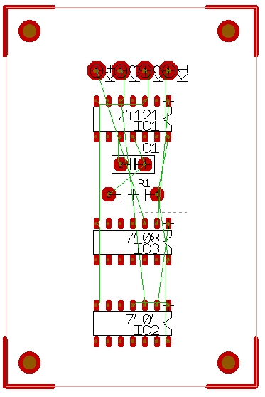
Place now all packages as suggested each after another K2, K3 and K4 and the ICs 74HC121, 74HC04DIN and 74HC08DIN with DIL14-packages (you can also choose different packages e.g. SMD instead of DIL). You can rotate the selected package by M2 before placing. Now only the resistor and the capacitor are left. Please pay attention to the real size of the components to be placed and soldered later. The figure x of the package namings Rx , Cx... mean the spacing between both of the connection pins, e.g. R4: 4-times IC-spacing of the pins of the IC (=10,16mm =400mil). According to tis the packages R1 and C1 are only suitable for an upright mounting. Place R und C close to the connections 10 and 11 of IC 74HC121.
Your PCB might look like this now:
Before starting the placement of the signal tracks, please note these ...
Remarks: According to the method of your PCB-manufacturing (etching or milling) special minimum widths and minimum spacings of tracks and soldering pads have to be realized. The following values seem to match well in both of the methods:
Power supply tracks (GND, +5V, Vcc, Us...) should show a minimum width of 1 mm (better more!). Place them first.
All other tracks should show a minimum width of 0,5 mm (better: 10,6 mm). The minimum spacing between tracks and respective to pads (aura) should amount 0,3 mm. The soldering pads of IC’s have in TARGET 3001! a standard size of 2,5x1,27 mm. So a spacing of 1,27mm between two pads results. Signal tracks, running between two IC-soldering pads may reach a maximum width of 0,67mm. Other pads, should have a minimum diameter of 2 mm (better 3 mm if space enough), connectors (e.g. soldering nails ): 4mm.
Setting of the soldering-pad size
Highlight by [Shift]+ M1 the components R1 and C1, then ![]() [e]
[e] ![]() Dialog: Edit the selected elements
Dialog: Edit the selected elements ![]() pads
pads ![]() Individual properties for the selected
Individual properties for the selected ![]() [OK]
[OK] ![]() Dialog: Change pads
Dialog: Change pads ![]() Pad height: 3 mm
Pad height: 3 mm ![]() Pad width: 3 mm
Pad width: 3 mm ![]() Drill hole: 0.9mm
Drill hole: 0.9mm ![]() [OK].
Don’t forget to tick the options!
[OK].
Don’t forget to tick the options!
Adjust the pads of K1 ... K4 to a size of 4mm with drill hole 1.3mm.
Note: According to this method you can edit any element of your project (lines, texts, signal tracks, pins...)
Placement of signal tracks
The placement of signal tracks on PCB by hand is corresponding to the placement of wires in the schematic mode. The air wires show you the pads to be connected.
Start with signal +5V or GND: ![]() M1 Draw track
M1 Draw track ![]() [o]
[o] ![]() Dialog: Track options
Dialog: Track options ![]() Track width: 1.2 mm
Track width: 1.2 mm ![]() track aura: 0.3 mm, 1 layer: 2 (copper bottom)
track aura: 0.3 mm, 1 layer: 2 (copper bottom) ![]() [OK]. Now highlight contact K1 by M1 and .... (see chapter 1.9 )
[OK]. Now highlight contact K1 by M1 and .... (see chapter 1.9 )
After placement of a signal tracks, the corresponding air wire fades. If the pad isn't hit in the right matter the airwire won't fade. In this case delete the signal segments starting from a pad and draw them new. As far as the space on your PCB is enough draw all tracks using the same width. If there are narrow spaces choose a smaller width.
Adjustment of signal tracks
Already placed tracks can be edited afterwards.
Those four buttons in this respect have a special meaning. ![]() Sidebar to the right
Sidebar to the right ![]() section "Settings":
section "Settings":
![]()
![]()
![]()
![]()
Select the desired highlighting mode and highlight the signal tracks you wish to change by M1 or [Shift]+M1. Single segments can directly be edited with M1 or displaced by M1H (e.g. for getting more space for placing signal tracks).
Can't hit superposed elements? Place the cursor close to the element in question and press [s] as long as the desired element flashes. Press enter to highlight it finally. Now press keyboard key [e] for edition.
With M1H you can open a catch-window above all desired elements. They get hightlighted that way.
Insert writings upon your PCB
You can easily insert writings upon any layer e.g. to point at certain connections or to drop other messages (data) on the PCB. On a single layer PCB as we have it here, only the copper bottom layer is used. So we drop our writings on this layer:
![]() [Drawing functions]
[Drawing functions] ![]() [Place texts] cursor transforms into
[Place texts] cursor transforms into ![]()
![]() M1 on this point where your text shall begin
M1 on this point where your text shall begin ![]() Dialog: Text options
Dialog: Text options ![]() insert desired text
insert desired text
![]() font height: min 2,5 mm
font height: min 2,5 mm ![]() font width: about 2/3 of the height
font width: about 2/3 of the height ![]() layer: 2
layer: 2 ![]() activate "mirrored"!!
activate "mirrored"!!
Check by the colour (normally dark red) whether the text really is placed upon this copper layer. Did you work out all the mentioned actions, your PCB could look like this:
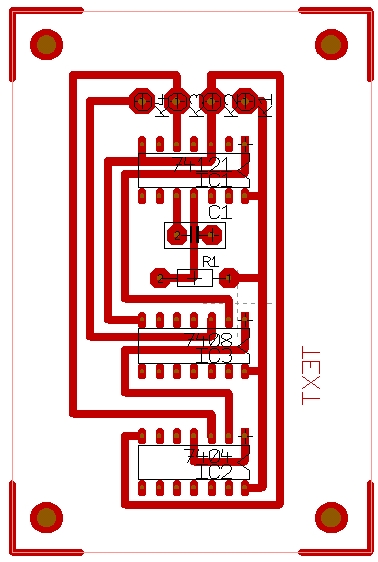
Check project
Now you can make TARGET 3001! check your project (schematic and PCB) concerning the design rules (Design Rule Ckeck). It is useful checking especially the track width and the spacings between the tracks and pads, as well as the check concerning not connected signals and short circuits (crossing tracks).
![]() File
File ![]() Check project...
Check project... ![]() Dialog: Check project - change only the parameter Track width to 0.5mm and let all other parameters remain at predefined value.
Dialog: Check project - change only the parameter Track width to 0.5mm and let all other parameters remain at predefined value.
The spacing between each of the signals and the thickness of the rest ring at pads should be bigger than 0.3mm. But especially when using IC’s lower values can often not be avoided. Start your check with ![]() [OK]
[OK] ![]() project checked.
The appearing list shows all errors and additional results of the check. For interpretation of the errors click M11 upon the purple coloured error flags (visible as far as the error-layer 29 is activated). Inactivate layer 29 so the error display is switched off.
project checked.
The appearing list shows all errors and additional results of the check. For interpretation of the errors click M11 upon the purple coloured error flags (visible as far as the error-layer 29 is activated). Inactivate layer 29 so the error display is switched off.
Output of a file for engraving isolation channels in HPGL-format
a) ![]() File
File ![]() Input-/Output-Formats
Input-/Output-Formats ![]() Production
Production ![]() Engraving isolation-channels
Engraving isolation-channels ![]() TARGET 3001! isolation milling
TARGET 3001! isolation milling
b) Follow the dialog to be guided through the process (double sided layouts work very convenient also).
Output of GERBER Data
a) ![]() File
File ![]() Input-/Output-Formats
Input-/Output-Formats ![]() Production
Production ![]() (X)-Gerber and drill output PCBout...
(X)-Gerber and drill output PCBout...
b) Follow the dialog, the Gerber data are generated to a directory of your choice.
That’s it.
If you have further questions, feel free to contact us.
