Solder stop
General
"Solder stop" in TARGET 3001! is also called "Solder resist, "solder mask" or "solder varnish". It is a varnish to avoid solderability at a special point. Only soldering pads are kept free of the solderstop varnish to allow solderability. The use of solder stop helps reducing the solder on the one hand and helps avoiding shorts caused by rests of solder when creating fine structured designs.
Normally every pad and via is automatically free of solder stop, meaning it is masked out from the solder layer and thus it is solderable. But if you want, you can have every single pad or via covered with solder stop too. Have a look at the dialog "Pad".
Solderstop in TARGET 3001!
A solderstop mask in TARGET 3001! by default is defined on layer 4 (solder mask bottom) or on layer 18 (solder mask top). The important thing is that the display of objects on this layer is inverted. An object displayed in green means: "Here is NO solderstop"! Thats why all pads appear in green if you switch all layers visible (including the solderstop layer).
Pads suddenly in green
Normally all standard components come in from the library uncovered with solderstop (=green) but this layer by default is not faded in. Tick the coloured box in the layer tool for fading in layers 4 resp 18 and see what your layout shows. All which appears in green has NO solderstop. If you want to make a certain area free of solderstop, please draw upon the solderstop layers the coresponding solid figures. They will appear in green.
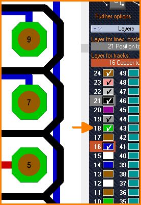
Release an area from solderstop
If you want to release a figure/area from solderstop, please draw the same figure upon a solderstop layer using the drawing functions. The figure which is free of solderstop varnish will appear in solid green.
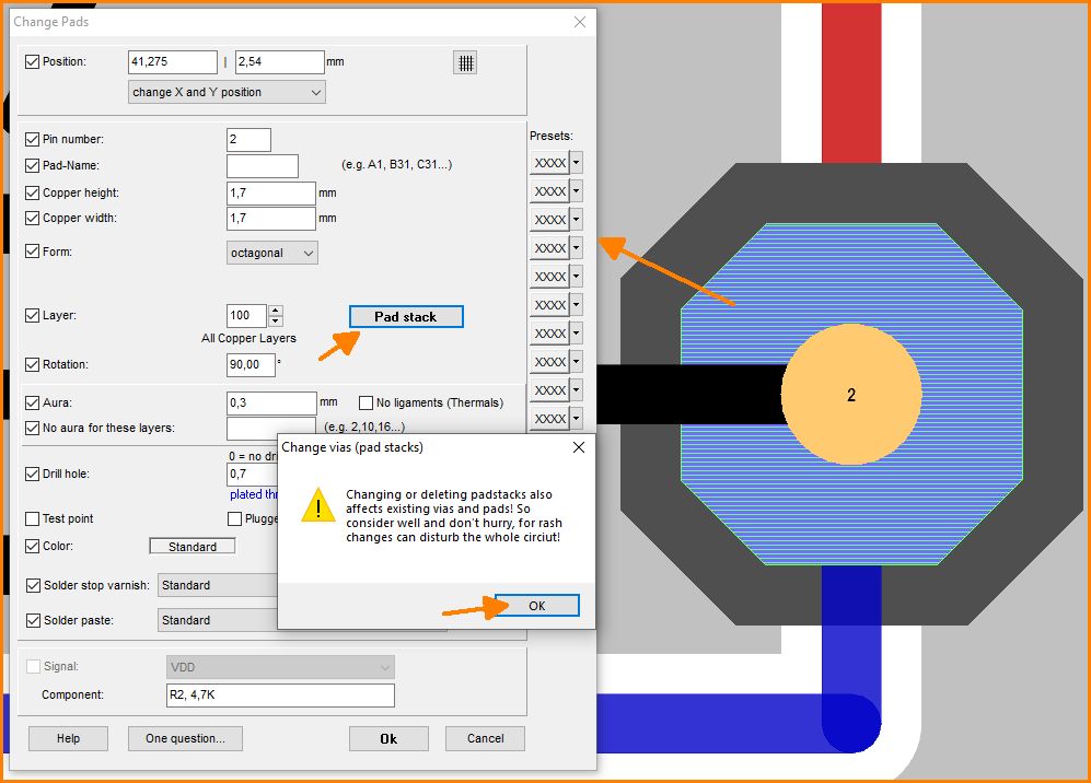
Give individual commands regarding solderstop varnish in dialog "Change pads". The dialog opens by double click M11 on the pad or entering key [e] for edit after having highlighted the pads.
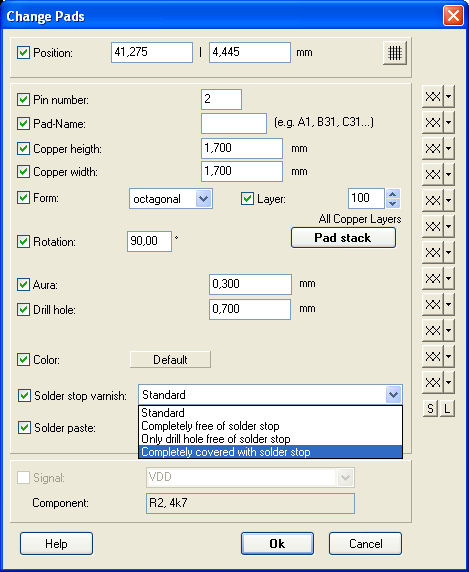
Widen the solderable area around all soldering pads
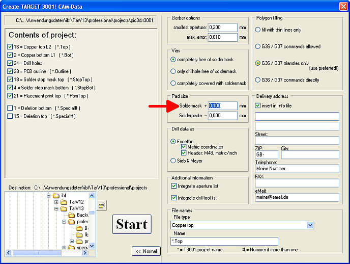
this means making the soldermask as a whole wider than the pads measurements. See menu "File/Input-/Output Formats/Production/(X)Gerber and drill export PCB out". In the flashing dialog please press button "Special". Now the dialog widens and offers opportunity to give addition to the complete soldermask which means to widen the solderable area.
Widen the solderable area around one or few soldering pads
You can just enlarge any pad's solderstop image in terms of widening the solderable area. Just use the drawing functions (under the pencil-icon) and draw upon your desired soldermask layer. Place a slightly bigger square over the desired pad which will keep the covered area free from solderstop agens (green gets wider means the solderable zone gets wider).
Another idea is to create a padstack consisting of lets say layer 16, copper top and layer 18, soldermask top: During the creation of the set of layers being touched, you can define layer 18 to be a bit wider. Later you can give a command that all pads desired shall come out like the padstack you just had created.
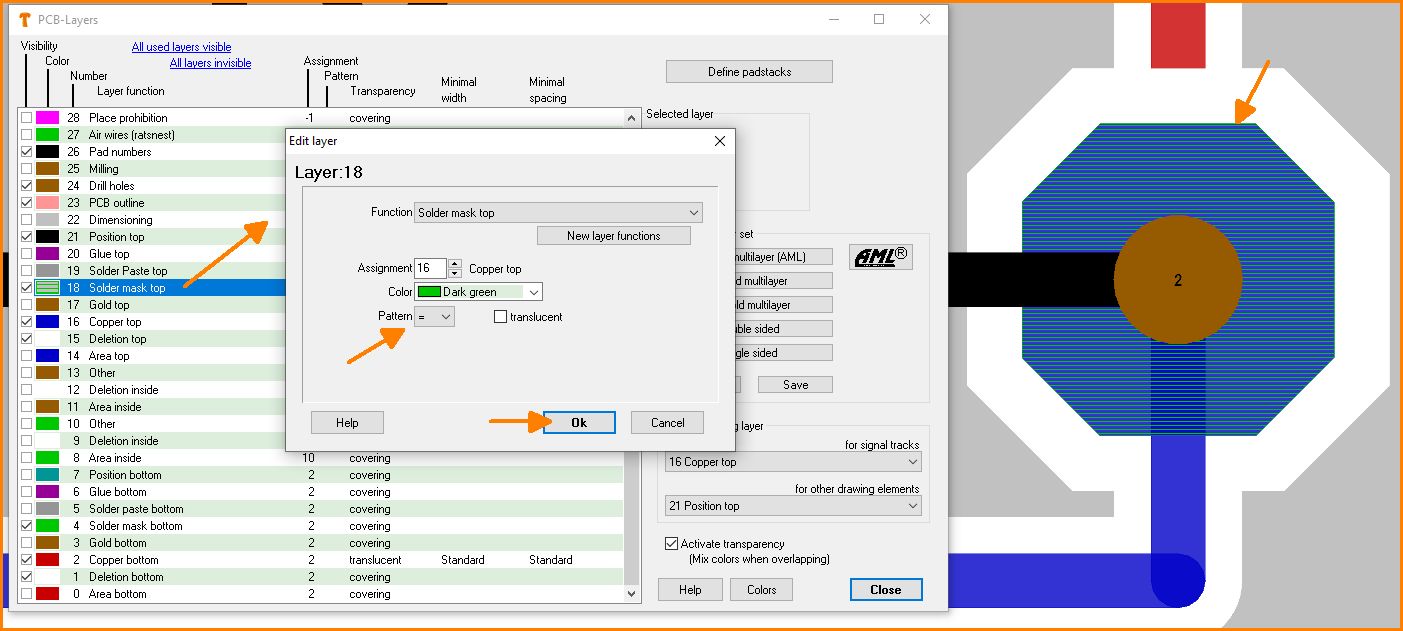
For creating a padstack, double click a pad and press button Padstack... in the flashing dialog. Prior to this set layer 18 to be displayed in line (= a pattern, thus not solid).
Then double click a pad and press button Pad stack:
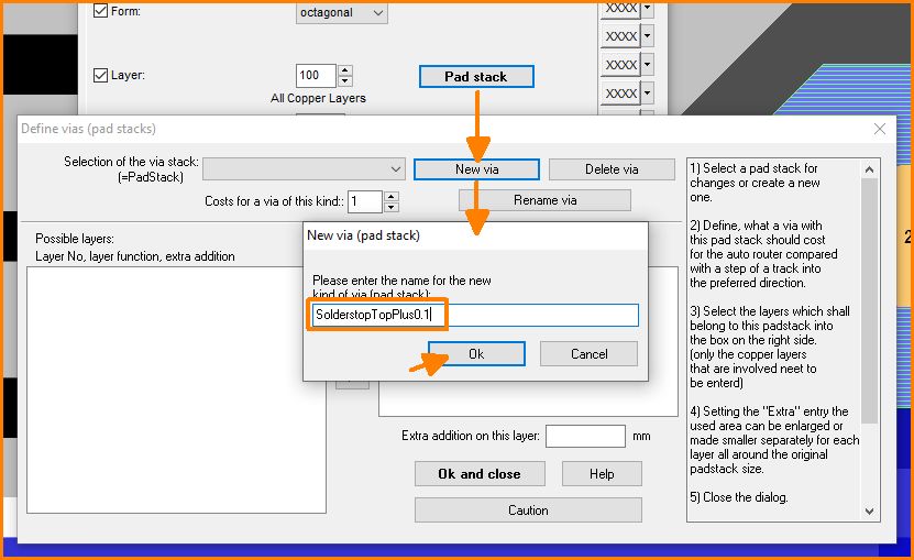
Now the dialog opens which allows to create a "New Via" what you now do:
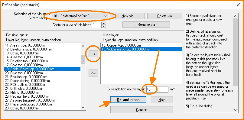
Now give it a name (e.g. coppertop_plus_0.1) and select from the list on the left each layer involved after the other by dragging it to the right side of the fields (use the middle arrow):
You see layer 16 and 18 have been dragged from the left to the right field. You see also in the upper oval the name of this kind of via we had given and the layer upon which it is defined (it's layer 101). You also see in the lower oval that you individually can give additions or subtractions to a certain layer. In our case 0.1 mm (use the comma as decimal separator) to layer 18, soldermask top. Now say OK and close.
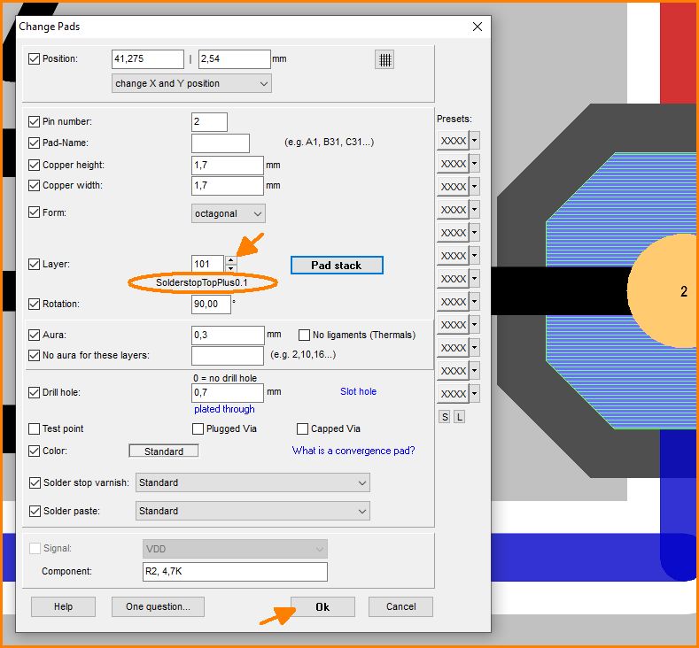
Now you return to the "Change pads" dialog which is still open and shows the a pad highlighted. Now shift this pad to layer 101 which is the defining layer for our padstack "coppertop_plus_0.1"
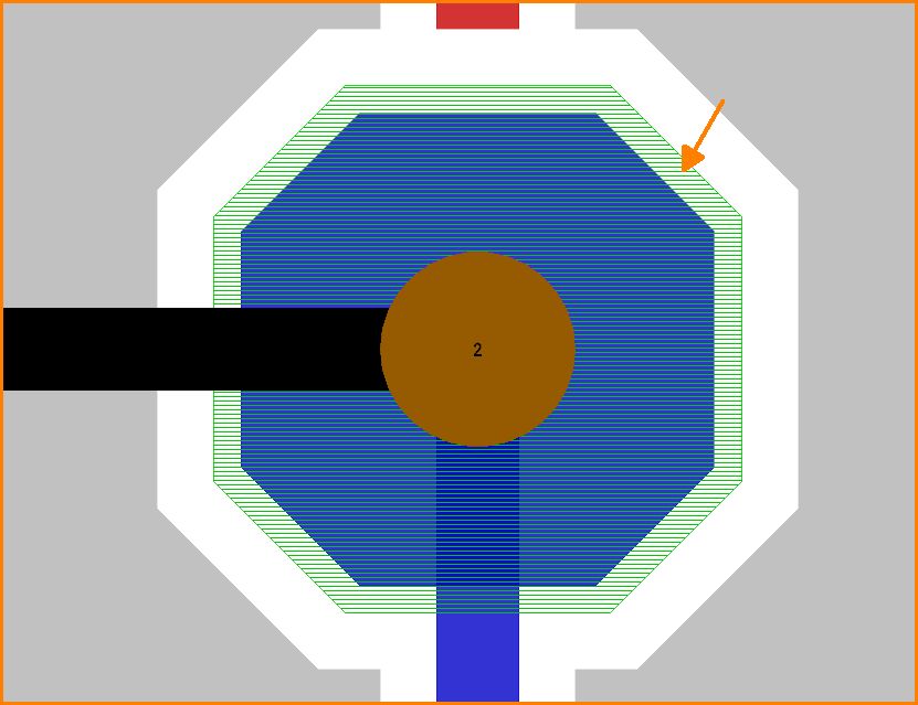
Press OK and see the result, the green (=solderable) is 0.1 mm wider than the pad itself:
All pads which shall come out this way please move towards layer 101, which makes them the way you had defined. You might check the result by the use of a Gerber viewer, e.g. GC Prevue from GraphiCode: http://www.target-3001.de/gcprevue.zip How to cope with it, please read in article GC-Prevue.
.
