Kinds of packages
After having drawn the schematic you'll be about to create the layout. The landpattern of packages need to be imported into the layout. The differnt housings vary in respect to their functions. From the soldering view they can be divided in wired and unwired (suface mounted SMD). Wired device need a galvanized drillhole for being soldered. The leads get pushed through the drillholes from the mounting side (top) and get soldered from the bottom side. Unwired device get soldered upon the top side of a board (Surface Mounted Device, SMD). By default components get positioned on the top side in TARGET 3001!. Also a positioning on the bottom side, the soldering side, is possible. When you tick the box "Autoplace the package directly on the PCB" in the Library Browser the components of the standard library are placed on the top side in general. They can be flipped to the bottom side (and back) by the use of the "mirror" function.
Examples for housings:
Resistor:
| wired | SMD | SMD |
|---|---|---|
 MELF (Metal Electrode Leadless Face) |
 Chip-cube |
Diode:
| wired | SMD |
|---|---|
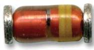 MELF (Metal Electrode Leadless Face) |
Capacitor:
| wired | SMD |
|---|---|
 Ceramic |
 Chip-cube |
Film |
 Tantal-SMD |
 ELKO |
 ELKO-SMD |
LED
| wired | SMD |
|---|---|
 |
 |
Quartz crystal:
| wired | SMD |
|---|---|
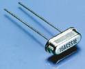 |
 Chip-cylinder |
Transistor:
| wired | SMD |
|---|---|
 |
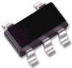 SOT (small outline transistor) |
Socket:
| wired | SMD |
|---|---|
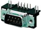 Sub-D |
Clamp:
| wired | SMD |
|---|---|
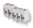 Clamp |
IC:
| wired | SMD |
|---|---|
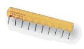 SIL (single in-line) |
|
 DIL (dual in-line) |
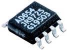 SO (small outline) |
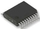 SSOP (shrink small outline package) | |
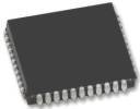 PLCC (plastic leaded chip carrier) | |
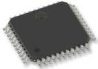 TQFP (thin quad flat package) | |
 BGA (ball grid array) |
An overview of various electronic device and their housings including additional links please find here: http://en.wikipedia.org/wiki/Electrical_element
.
