Import Package
Importing a package means bringing the solderable footprint pattern to the PCB layout. When drawing a "New PCB with schematic", packages are assigned to symbols in the sense of a Package proposal. When drawing a "New PCB without schematic", you can use all packages in the sense of a free package. "Free" means free from being proposed to a schematic symbol. Sure you can use free packages in the "New PCB with Schematic" mode if you'd like to deviate from the package proposal.
To import a package:
- select in layout Menu Package / "Import Package"
- press directly the [INSERT] or [e] key
- select the icon

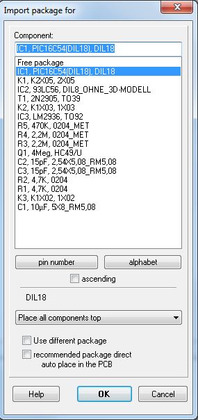
Coming from the schematic a package will be suggested. You can select each package from the list of proposals which is result of the schematic symbols in use (for example: for IC1).

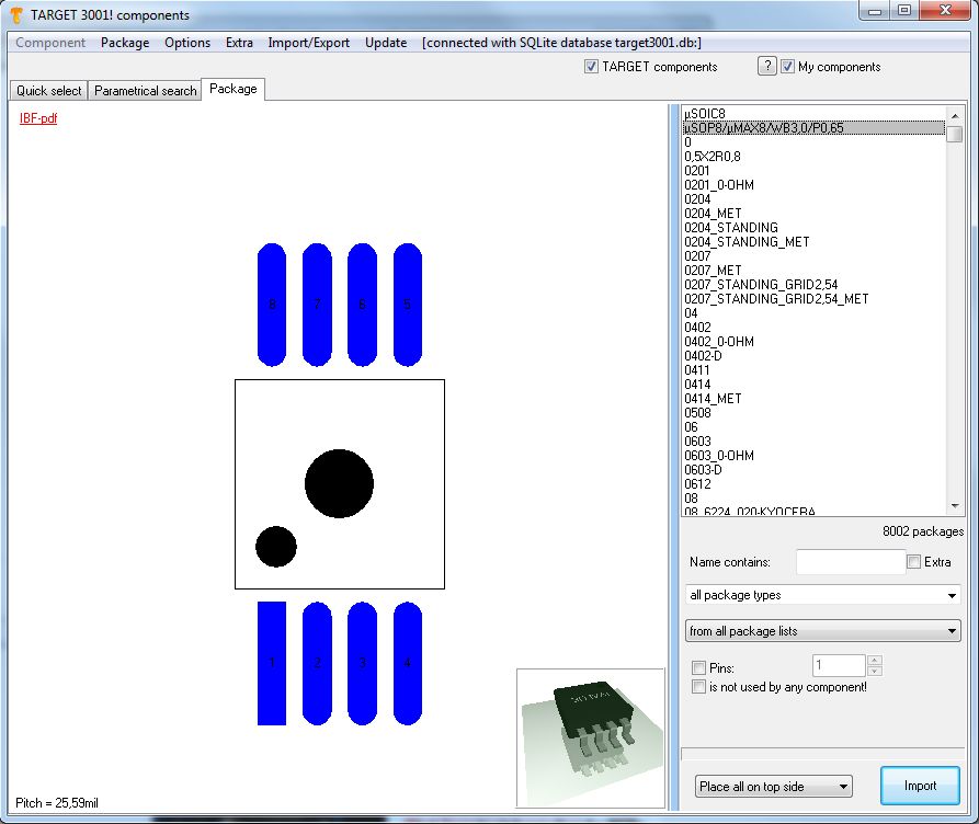
In case you wish to deviate from the package proposed, you might use a free package (a package with no reference to the schematic). A dialog will appear to select the desired package from the list. Also use the line "Name contains:" in order to use catchwords in the component name. Ticking the "Extra" box searches in the component description as well:

Image: The dialog in the component data base to select a package.
If you use the project kind: "... without schematic" this dialog opens as well when intending to import a package.
In most cases, you can confirm this suggestion with OK. You should only enter to this dialog if you are sure that you need a completely different package (for example: SMD16 instead of DIL16). After you confirmed this import dialog, the package will be placed on the PCB. The package outline is attached on the cursor and can be placed M1, or rotated with M2. Get rid of it by M12 or "Escape".
Components in TARGET 3001! come from the data base generally meant for being mounted on the top layer. Those non-smd ones are meant for being soldered from the bottom side. You initially view them by blue footprints. Blue is the default color of layer "16 Copper top". Because you always have a view from the top layers through all other layers to to the bottom layer. If you fade out layer 16, you will see the footprints in red. That means a conventional pad looks that way:
From which side you lead a signal track on it, depends on you. A pad can be a conventional one (going with a drillhole through all layers, being tinned at the inside and having the same shape on the top side and on the bottom side) or a SMD one located either on the top side (blue) or on the bottom side (red). Bringing a component to the opposite layer is very easy: flip it by mirroring! Use the key [m] after having highlighted it. [m] is for a horizontal mirroring, that means the mirror axis is vertical. [Shift]+[m] is for a vertical mirroring that means the mirror axis is horizontal. Please note that the cursor position defines the location of the mirror axis. So do not move the cursor too far away from your desired package when mirroring. You might flip it out of screen. You will recognize by the change of colors of the pads that you brought it to the opposite layer. Play a bit with it, and you will see it is easy!
If a text element belongs to a package drawing, the following names will be exchanged: The name !COMPONENT or a text saved as the component name, will be exchanged with the component designator (IC1, R1); the name !VALUE or a text saved as the component value, will be exchanged with the component value (4000, R). Package import.
If you wish to transport a component e.g. by eMail, please note:
only databases can be transported, single components can't. This means you need to export the component to an individual database. In consequence this database might have only one component.


