Reorganisation
![]() and
and ![]() , also see menu Actions/Reorganisation or menu File/Reorganisation
, also see menu Actions/Reorganisation or menu File/Reorganisation

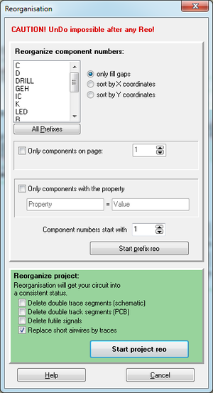
Reorganize component numbers (prefix reo): all component types having a component value which can be renumbered/reorganised are listed within the listbox. E. g. you are placing resistors. Their prefixes (R1, R2, R3...) get numbered by TARGET 3001! automatically. For electrical reasons you later decide to delete resistor R2. The resistors R1 and R3 remain in the schematic. Now that's the point where the prefix reo is used for rearrangement. Select the prefix "R" in the list and then press button "Start prefix reo". Now all resistor prefixes get renumbered starting from R1. Thus R3 becomes R2. If needed please also highlight those prefixes, whose components shall get renumbered. The renumbering also can be done in the layout following x- or y-direction. In case a component does not have a package currently the schematic coordinates unfortunately are not used for assorting.
- Only fill gaps: all prefixes of all components placed get renumbered.
- Sort by X coordinates: prefixes get renumbered in x direction.
- Sort by Y coordinates: prefixes get renumbered in y direction.
The assorting in x or y direction might be useful when searching errors in the layout or in case you do assembling by hand. The assembling person immediately finds the location on the board where to place the device. This kind of assorting only works by layout coordinates. If a component exists only in the schematic, it is not part of the re assortment.
The project reorganisation (green area) is an action for cleaning up the internal memory. Remember: when using the undo- and redo function deleted elements are still in memory available. Thus memory space is used, even if the elements are not visible. The "Reorganisation" command deletes these elements from the memory. A undo or redo action afterwards is not possible any more. If a component consists of more than one symbol (eg IC1a, IC1b, ic1c...) those parts of symbols which are not yet used in the schematic, will not be deleted (for example if only IC1b is in use, IC1a will not be swept away, even if it has been deleted from the schematic).
The PCB is clipped to 2m x 2m. Additionally all signal names which were given automatically are rearranged and enumerated new: Sig$1, Sig$3, Sig$4 become Sig$1, Sig$2, Sig$3).
The "Reorganisation" also wipes out unused signal names. The PCB will be resized to 1,2m x 1,2m area. The reorganization can also rearrange the order of the names of components to be populated. The renumbering can take place towards X-dierection or Y-direction of the components in the circuit board.
Please Note: If you delete a schematic symbol, even if the corresponding package still exists on the PCB, this schematic symbol will not disappear from the list after a "Reorganisation"! In case orphan airwires appear in the layout, a reorganisation helps to wipe them out.
Please Note also: The project-reorganisation is meant for projects only. Pads with pin numbers not belonging to a package are no valid members of a project. So they are changed to "mounting hole" pads. Therefore please do not execute a project-reorganisation during component design. Whereas loading and saving a project with a component that is just coming into being does no harm.
A similar thing happens to symbols which are just created with [y] but not exported with [x] yet. These symbols not being members of a component are extinguished, as they are not belonging to a valid project.
.

