Multilayer
What is a multilayer?
Imagine a multilayer PCB as a sandwich made out of two or more double sided PCBs glued over each other. As a result you have inner layers, which can be used for signals. You can set vias to connect the inner layers (buried vias) or vias to connect outer and inner layers (blind vias).
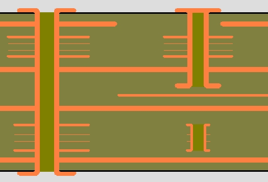
See the sketch of a 16 times multilayer showing the principle of a through hole, a blind and a buried via:
How to set that up in TARGET 3001!
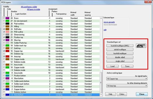
In TARGET 3001! you can easily set a four or sixfold multilayer configuration by pressing one of the default buttons in the layer tool:
You also can set it by hand: for a fourfold multilayer in TARGET 3001! set the function of layers 10 and 13 from "Other" to "Copper inside". If you need more layers, please set further layer functions to "Copper inside". You can rearrange the whole set of layers, if needed. Do the following:
- open the layer tool in the tool bar above
 and double click layer line 10.
 - in the opening dialog set the layer function from "Other" to "Copper inside".
- double click each layers 8, Area inside and 9, Deletion inside.
- Set the assignment of all three layers to 10 (= Copper inside).
Do the same with e. G. Layer 13:
- open the layer tool and double click the layer line 13.
- in the opening dialog set the layer function from "Other" to "Copper inside".
- double click each layers 11, Area inside and 12, Deletion inside.
- Set the assignment of all three layers to 13 (= Copper inside).
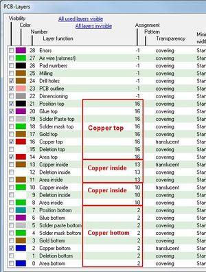
Image: Layer setup for a fourfold multilayer
Further inner layers can be created the same way. Take care to establish a layer with function "Copper inside", "Area inside" and "Deletion inside". Those three layers need to be assigned to the number of the "Copper inside" layer. It is because a ground (or any other electric potential) -plane which shall appear on this copper layer needs an area which is defined on the area layer. The same with the deletions which represent the auras = spacings of the tracks to the plane. They are put to the deletion layer. Now both layers need to be assigned to the copper layer number they are meant for. This is the sense of the "Assignment".
How to cope with vias, blind and buried
If you wish to use blind vias (expensive) and buried vias (more expensive), you must define Padstacks in Menu Actions / "Define Vias as PadStacks". Now you are able to create those special vias on layer 101 ff. On Layer 100 those vias are defined, which contact all copper layers, e.g. a galvanized drill which is technically the same like a galvanized via.
If you press key [.] in "Draw track" mode (as if to set a normal via) and then key [o] for "Options" then configurate several vias in the "Via-Options"dialog on to the buttons on the right edge of the dialog. Use button "PadStacks". Those buttons later appear also beneath the layer tool for a quick selection while placing tracks.
If you need further information on the capabilities of multilayer technique, please contact also your PCB manufacturer. Sure they can provide information on their multilayer processes.
Multilayer in 3D
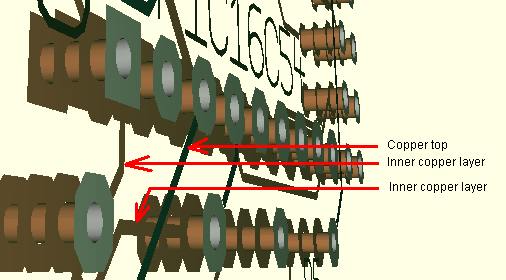
In 3D view you easily can see the separate tracks upon separate layers (though it's a bit difficult to figure it out in this 2D screenshot):
Multilayer setup for testing
This TARGET 3001! project has a multilayer configuration: Pic_4Multilayer.T3001
