Insert image
Inserting an image into the schematic
You would like to have a logo or similar in your schematic, for documentation purposes or to give your drawing a special look. You should have a corresponding image at hand. Supported image formats are BMP, GIF, JPG, JPEG, PNG, TIF, TIFF.
In our example we use the TargetLogo200weiss.jpg.

Image: This image is to be printed in schematic and layout.
The file format of the above image is *.jpg in a size of 200 x 63 pixels. The higher the resolution, the sharper the image in the project. It is up to you which resolution and dimensions you use. Experience has shown that the images used are small, because in most cases a logo shall be placed at a certain position.
To insert an image, use the menu item: Actions/Insert image.... The following dialog opens:
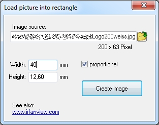
Image: The dialog "Load picture into rectangle"
Now select the desired image from your directory. Before that, you determine in the dialog the size in height and width, just as you want it to be in the schematic. If you set the check mark to "proportional", then you only need to determine either the height or the width. The other value results automatically from the dimensions of the image. Click on the button "Create image" in the dialog. The lower left corner of the position frame now is fixed to the cursor and can be dropped with a mouse click.
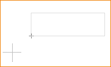
Image: Position frame (=a bounding rectangle) of the image
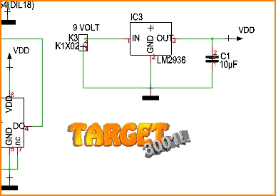
Image: The desired image is inserted to the schematic
A new click on the picture will highlight the image with black touchpads at the corners and in the middle. Holding one of these, you can stretch or compress the image. If held at a border line segment, the whole image can be moved. Double-clicking on the picture opens the dialog "Change rectangles". This refers to the rectangular border around the image. If you change the rectangle height and width in this dialog box, the size of the image will change accordingly.
Inserting an image into the layout
Print on paper
In the layout view, proceed as described for the schematic, the function is identical.
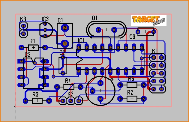
Image: Logo inserted for a paper print of the layout
If you print your layout with logo on any printer, you will get the following picture:
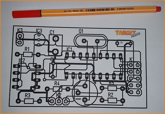
Image: Logo in a paper print of the layout (300%)
Print (relief) of copper
No Gerber data can be created from colored images on layouts, nor can they be displayed in Postscript. If you want to display the contours of a logo on your printed circuit board in copper (or on a front panel in aluminium), it is best to have your logo as a high-contrast bitmap (*. bmp) in sharp black and white, like this:

Image: TARGET-Logo black and white (Note: For loading speed reasons this picture is a *. png, not a *.bmp. To have it made as a relief in copper you need the bitmap format.)
Now you have to generate this bitmap into the database like a component package.
Select menu item:
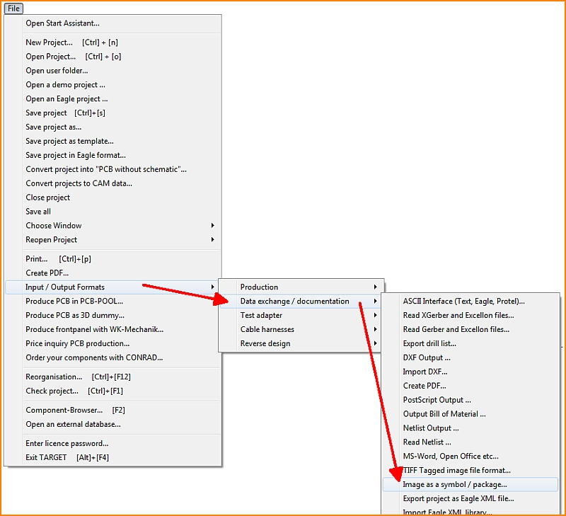
Image: Menu path to create an image as a symbol or a package
Load the black and white bitmap by the dialog box that opens.
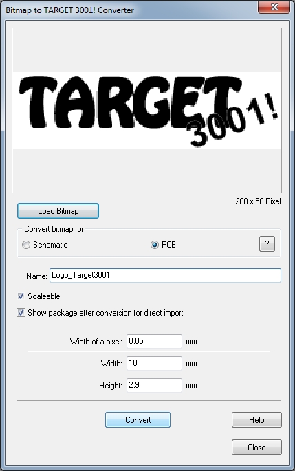
Bild: Bitmap-to-Target converter
By clicking on the radio button you can define that the bitmap should appear in the board, i. e. in the layout in the sense of a "package". It is also possible to create the image for the schematic, in the sense of a "symbol".
Our image has a width of 200 pixels. If we determine a pixel with as of 0.05 mm in TARGET, the real size of the logo on the PCB will be: 200px x 0.05 mm/px = 10.00 mm (one centimeter). After conversion of the image, the package browser opens and offers us the image for an immediate import into the PCB.
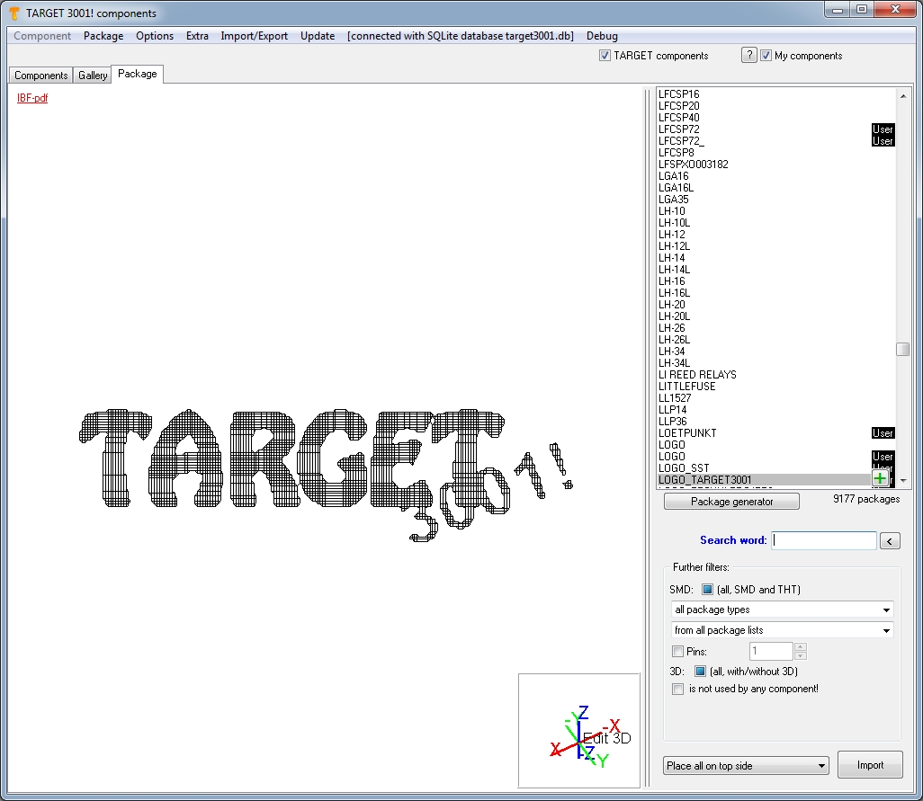
Image: The package dialog immediately suggests the import of the logo into the layout.
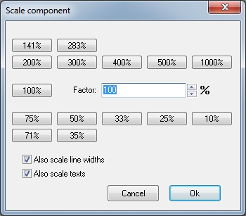
Image: Scale component dialog: We take over the image at 100%, thus non scaled.
The image now is fixed to the cursor and can be placed anywhere on the copper side that is currently activated. In our example layer 16, copper top, blue.
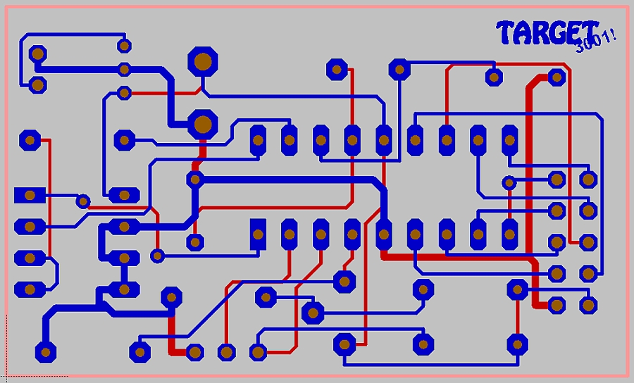
Image: Layout with TARGET Logo on layer 16, copper top, blue.
If you want to have it on copper bottom, i. e. layer 2, copper bottom, red, you just have to mark it and mirror it with keyboard key [m]. The mirror axis is the cursor position. So move the cursor in the middle of the logo when mirroring. If you move the cursor too far away, the image might move out of screen. You can select it at any time and move it with mouse key held.
If you now create a ground plane over the whole board on layer 16 (menu: Actions/Ground planes/Entire PCB area...), you will get the following picture:
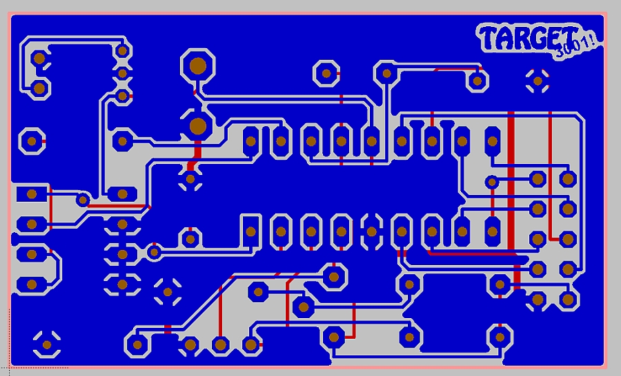
Image: Copper logo embedded to a ground plane
As deletion from a copper plane (as an omission)
To do this, you should have created a ground plane on the copper layer in question. Now simply bring the logo to the appropriate "Deletion"- layer . So in our case it is layer 15, Deletion top.
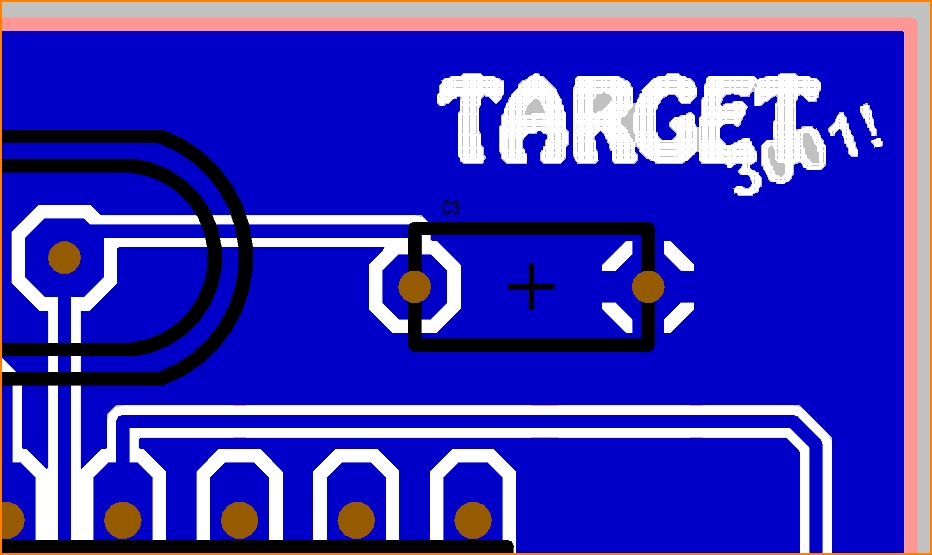
Logo brought to the deletion layer.
The more filigree and delicate your image is, the more difficult it is to let copper flow around it. Keep in mind that Gerber data is the basis for a light exposure process. Light pens, which move according to the tracks of the the layout upon a photo-sensitive plate, always have a certain line width (=aperture). If this line width is too large or cannot be reduced in terms of production technology, the tools do not work well in all corners. More than that orphan ground areas (signal islands) are left out completely if necessary. The results then are not convincing. In addition, deletions from a ground plane can always cause electromagnetical irritations. We therefore tend to advise against this method.
Alternatively, you could place a rectangle in the delete layer and then again put the logo in copper on it.
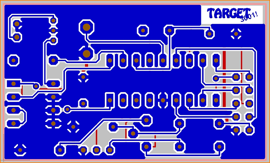
Logo in copper drawn on a rectangle of deletion
Using an image as a design template
A photo of an existing PCB design
Guess you have no layout data from a previous project but only the PCB physically in your hands. Now you would like to reproduce the board and have the idea to import a picture of your PCB like a "drawing template" into your layout to place components and traces piece by piece. It's very easy. Please read more in the article Reverse Engineering.
Image data (DXF) of a board outline
Please refer to the article DXF where the import of DXF-data is explained.
Engraving a logo on a front panel
You can read more about this in the article: Engraving a logo to a frontpanel
The process is identical. Simply exchange the copper layer by a frontpanel layer (not milling but engraving).
