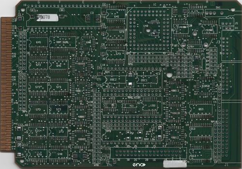
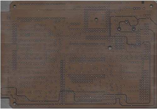
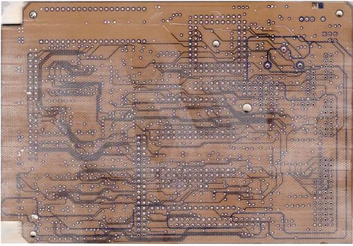
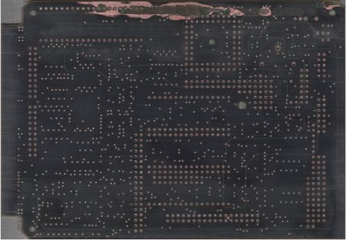
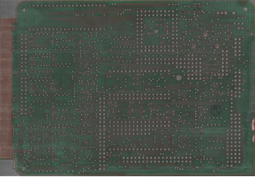
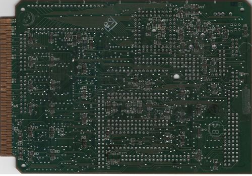
Reverse Engineering
The problem: You have an old, defective circuit board without any documentation. Also CAD data are not available. Unfortunately this circuit board controls a bucket wheel excavator, a rail bus, a ferry, an airplane, a locomotive, a rack railway or other large equipment, which is unproductive because of that electronic damage. The manufacturer himself hasn't existed for years, and service companies are not on the spot. If you don't want to scrap the whole system sooner or later, the only option is to rebuild the circuit board. Even for an experienced layouter this process is a real challenge.
The solution: Redraw the layout in TARGET 3001! and use it as a "logic primitive" for a schematic to create. Let TARGET help you generate a schematic from it including the respective part names and signal names. Now a new PCB layout can be derived like a "clone" from the old one. This feature was developed in conjunction with Fraunhofer IPK and ENA Electronics. ENA are also a service partner for customers.
 |
We recommend this book on Reverse Engineering. Various steps had been made using TARGET 3001! Find it at Amazon. |
Reverse bound constructing
The idea is to shoot an image of your existing board and import it into TARGET. A picture is just a painting and its parts have nothing to do with conductive tracks, solder pads or ground planes. These elements have a multitude of circuit-related properties. But an image of the circuit board as a template is a great help. You simply place the image "underneath" your layout and place the elements exactly on top of this projection. You can insertt images from top and bottom side into your layout with semi-transparent congruence. Then you lay the tracks. Later you can derive a schematic from it, if needed with several schematic pages. At the beginning, always select the project type "without schematic". A schematic is derived later from the finished routed replica.
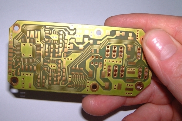
Image: A hardware circuit board, without any documentation, or even CAD data.
Load the normal view of your bitmap (image format *.bmp) on layer "14, area top" and place the component packages (solder pads), traces and other layout elements on layer "16, copper top". In addition, you can insert an image of the bottom side of your layout mirrored on the horizontal axis into TARGET on layer "0, area bottom". With the slider "transparent...opaque" in the dialog "Load image into rectangle" you determine the opacity of an imported image. For example, you can look through your "Copper top" photo to see what is going on in your "Copper bottom" photo. This makes it easier to place packages and tracks exactly on both sides.
First, make sure that the dimensions of your screen display (in mm) are correctly set in the Settings/Options menu. Otherwise unwanted distortion of the bitmap may occur.
Build up the layout
Prepare an image of the existing board
1. step: Create a bitmap of the board you want to trace in TARGET 3001!, scan or photo. Measure the side lengths of your real board. This sample board has a height of 43.00 mm and a width of 90.00 mm. We ignore the cut corners for the moment:
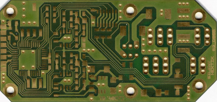
Image: Scan of the board in format Bitmap *.bmp
Select project concept
2. step:Open TARGET 3001! and select the project type "Double-sided PCB without schematic", no matter if you want to derive a schematic later or not. If you intend to only have a single-sided board, please select "Single-sided PCB without schematic". In the layout view now draw a board outline upon layer 23, Outline, with exactly these dimensions. Let the PCB Outline Wizard assist you (see Layout menu Actions/Automatisms and assistants/PCB Outline Wizard).
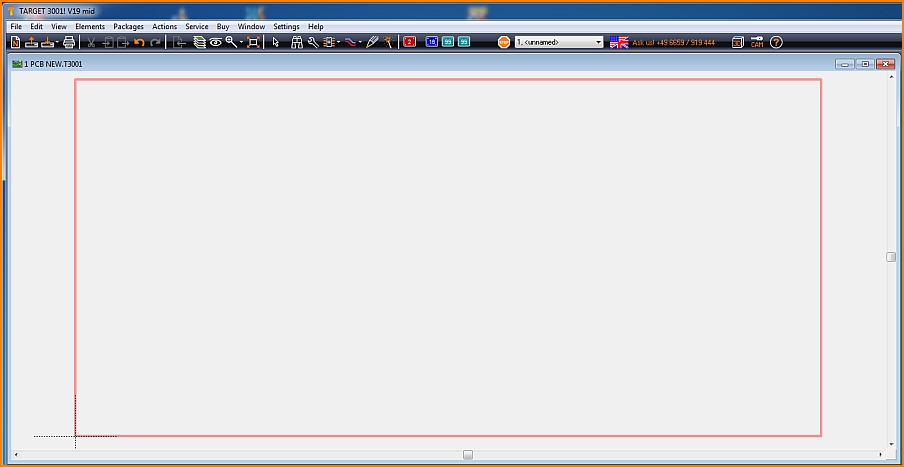
Image: Board outline in TARGET showing identical measurements of hight and width
Insert image
3. step Open layout menu "Actions/Reverse Engineering/Insert image behind board"
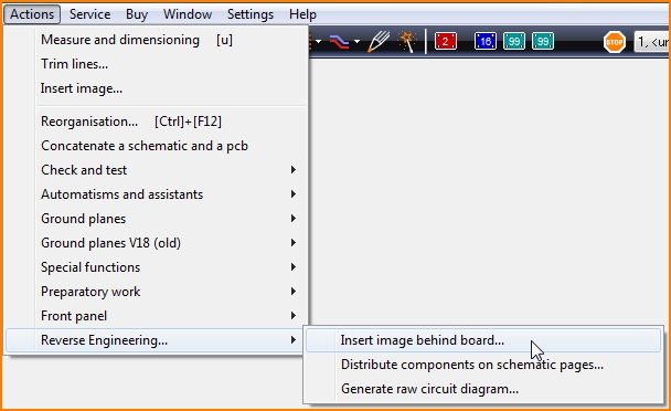
Image: Start Reverse Engineering
The image can automatically be fit into the board outline:
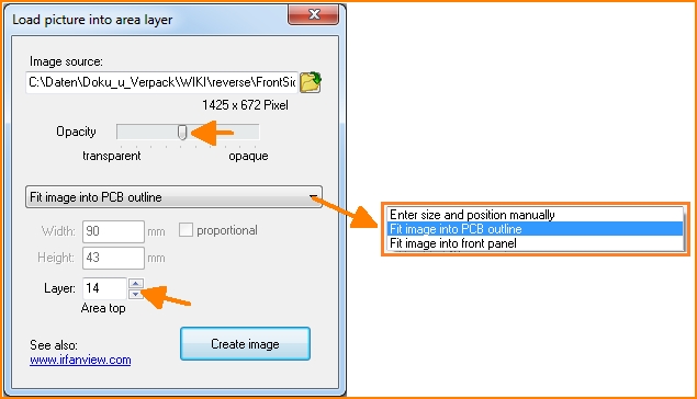
Image: Fit image into board outline (from V19)
A larger image is "reduced" to the dimensions of the board outline. A smaller image is enlarged accordingly, but can then might become pixelated. In our example we see the component side (upper side) of the board. We can import the image as a template on layer 14, Area top. In the image import dialog we determine the layer for this image. Nevertheless, the image can be moved to any layer later by double-clicking on it. You now can miter the corners of the outline (light red, layer 23, PCB outline), but you can also do this at a later time (highlight the outline and click M2 on a black little touchpad of a corner. Now see the context menu for mitering).
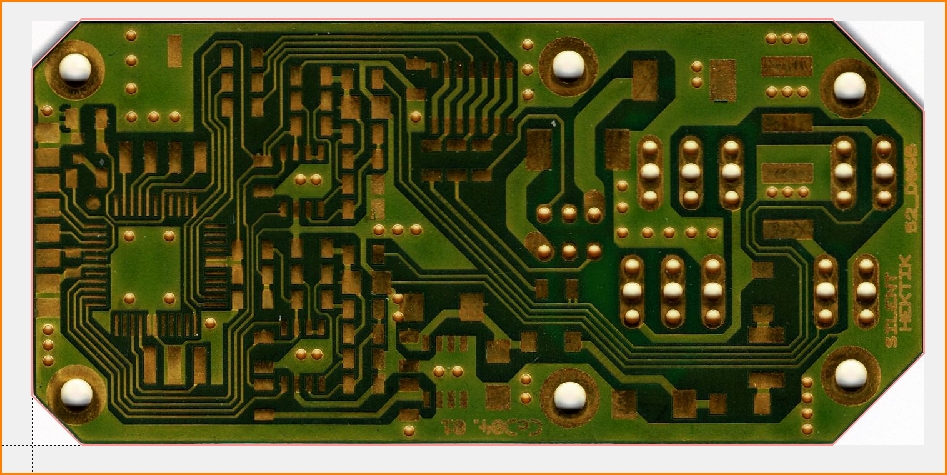
Image: The component side of the PCB fit into the outline.
Repeat the process to additionally display an image of the bottom side of your board on layer 0, Area bottom. If you reduce the opacity of the image of the top side (see dialog, which you open by double clicking on the image), the image of the bottom side can shine through. When redesigning, i.e. "redrawing", the top and bottom sides can be viewed simultaneously.
The bottom side of your board looks that way:
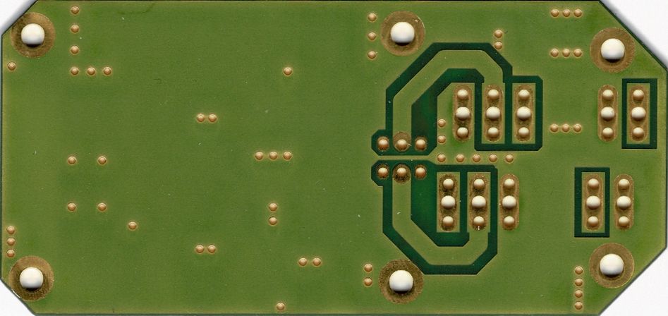
Image: A photo/scan of the bottom side of the board, mirrored on the vertical axis.
We now put this image on layer 0, Area bottom. Again see Layout menu Actions/Reverse Engineering/Insert image behind board. In the opening dialog we select layer 0 with full opacity. If we only fade in layer 0, Area bottom and layer 23, PCB Outline, the following image will appear:
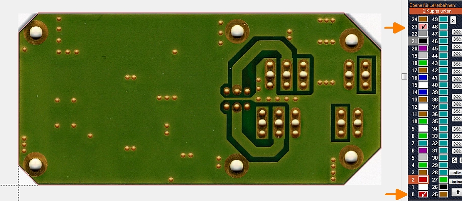
Image: In TARGET: Image imported to layer 0, Area bottom. Layer 23, PCB Outline, is faded in as well (light red line surrounding the board).
If you set the opacity of the board top image on layer 14 to about half using the slider, you can add layer 0 and get the following image:
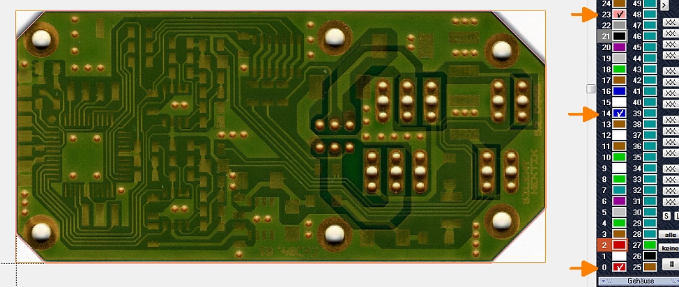
Image: Both images superposed to each other
Double-clicking on an image opens the dialog for image import or image manipulation, see above. Here you can also set the opacity. To grab a certain image, simply move the other image aside. After the changes are made, move it back again. Both images now can be seen. The image of the bottom side needs to be mirrored on its vertical axis. The upper image must have a certain opacity so that the lower image can shine through.
Import packages
4. step: Start importing the packages that were used on the layout from the database. On the left side of the photo we can see that a TQFP44 package was used. Get one from the TARGET parts database.
Important note: Don't get just any, bare standard package in to your layout. It lacks the schematic symbol. Get in a Componentpackage. Only a comonent package carries the significant symbol along which is necessary for the later import to the schematic.
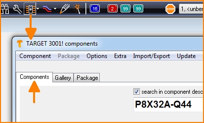
Image: Use TAB "Components" when importing a package. Don't use the "Package" TAB because a bare package does not bring a symbol along.
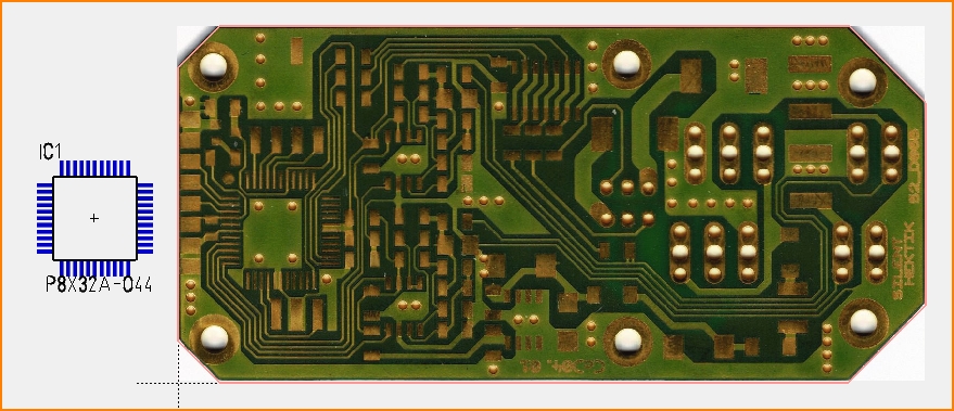
Image: In TARGET: A TQFP44 package taken from the component library by the package browser.
Place it to the layout. Zoom in as far as possible and place the package as precise as possible. Use the x-ray function (key [#] on your keyboard). Eventually set the grid smaller. All layout drawing functions can be used.
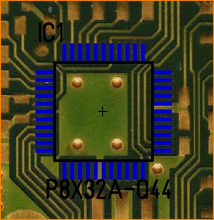
Image: First package exactly placed.
Placement of packages and signal tracks
5. step: Place e.g. an SMD capacitor 0805 and draw the tracks between the footprints in question simply by redrawing the structures.
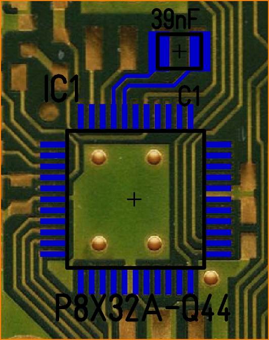
Image: Two packages placed and two tracks drawn
Now get each part piece by piece into your layout, place it and connect the contacts as shown. In our example you will see the results in blue as this is the default color for layer "16, copper top". If you want to edit the solder side (bottom) of the board, you have to load the mirrored bitmap of the bottom already on layer 0, see above. You look through the board from above to the bottom, as usual in TARGET.
Derive a schematic
Limitation in deriving a schematic from the layout
Important note: The following partly automated steps for creating a schematic from the layout are limited. Principle: Half the number of pins of the respective TARGET-edition. More detailed information can be found in the Product overview. Have a look in section "Reverse Engineering".
Are all component packages placed in the layout and are all traces routed?
6. step: If yes, the creation of a schematic from the layout structures, can take place. Once a schematic has been generated, all further development work for this project starts from the schematic. Reverse engineering is then no longer possible. The photos of your board have done their job and are no longer needed. They can be deleted. But you can do this later as well.
Distribute components on schematic pages
Please see menu: Actions/Reverse Engineering/Distribute components on schematic pages
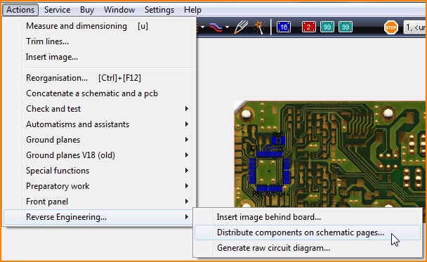
Image: Menu Actions...
In the dialog that opens, you see the list of component packages as they were used in the layout. At the same time you are prompted to click M2 on a component which you want to assign to a specific schematic page. A name must first be assigned to this schematic page. The schematic symbol will then appear on this page. In our case we call it "Processor", any name is possible. In the following intermediate dialog you confirm the schematic page for the highlighted component. With the second component, the same principle: Right click on it and select schematic page or determine new schematic page name.
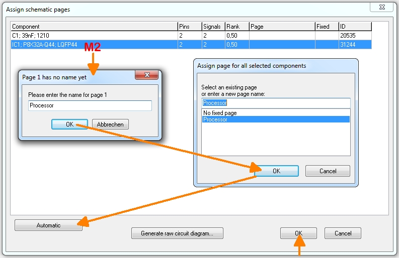
Image: Establish schematic pages by naming
Placement automatism in the schematic
If the project consists of a lot of components, the selection process described above can be tedious. The button [Automatic] helps here and assigns components that tend to belong together to the same schematic page. For the use of the automatism it is helpful to manually assign the "meaningful" components to certain schematic pages at the beginning. Usually those with many leads or with a key function within the circuit. The automatism then assigns the closely associated symbols to this schematic page as well. "The child wants to be close to it's mother" is how the principle could be described. A heuristic algorithm is used to distribute the components. Global signals, e.g. GND, are not as weighty in this respect as significant one-to-one connections.
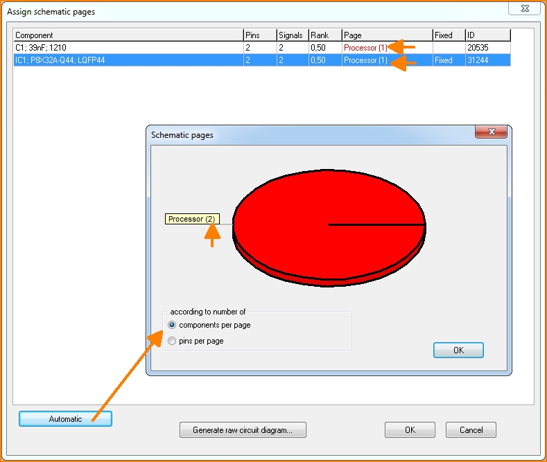
Image: Component distribution to schematic pages
A diagram shows the distribution on schematic pages by: "Components per page" or "Connections per page". Press OK to generate a raw schematic diagram.
Generate raw circuit diagram
Press the button in the dialog box (hidden in the image above) or select the menu item:
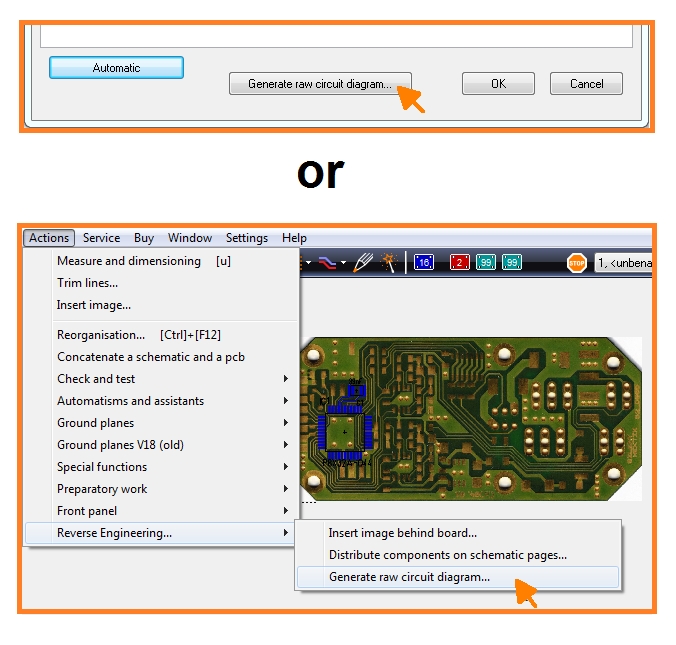
Image: "raw" means: There is something left to do...
The result shows the first schematic page with the part symbols and the signal connections as purple air wires.
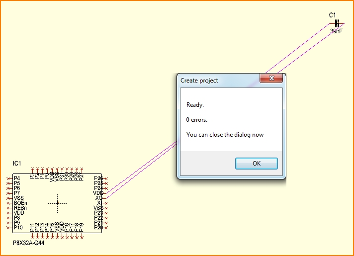
Image: A purple air wire has its origin in the PCB track
Touch the capacitor at the handle cross with the key held M1H and pull it closer. While pulling, click the right mouse button (M2) at the same time to rotate it. The purple lines are air wires. Signal wires must actively be established. Either by double-clicking on it to use the schematic router or by the tool: "Place wire [2]".
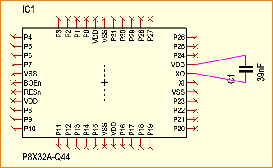
Image: Component brought closer and rotated
Signal placed: Once with the tool (above) once by double-clicking on the violet line or by selecting and pressing key [+] (schematic router):
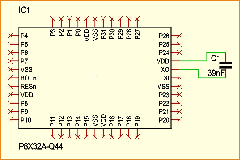
Image: Signals established and signal wires laid
Now you can handle each signal individually, edit it, redraw it... If you want to convert a signal back into a purple air wire, select it and type key [-].
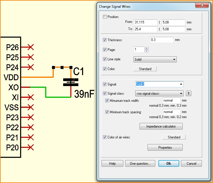
Image: Double click M11 upon a signal
More than one schematic page
If a signal appears on several schematic pages, a reference symbol is placed at the edge of the schematic page. This reference symbol indicates that the signal is continued on another schematic page. The corresponding schematic page shows an equivalent reference symbol which introduces the signal there. The following example shows this:

Image: The symbols of components can be predefined to appear on various schematic pages
In the "Assign schematic pages" process, IC1 was assigned to the "Processor" schematic page, while capacitor C1 was assigned to the "Power" schematic page. After "Generate raw circuit diagram" the IC on the schematic page "Processor" shows two purple air wires which lead to two reference symbols. At the same time the second schematic page "Power" is visible.
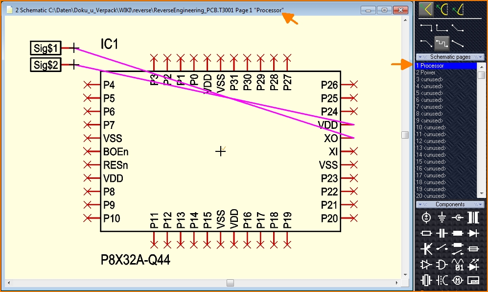
Image: The air wires in the schematic point to the reference symbols at the edge of the schematic page.
If you click on the second schematic page in the bar on the right in order to show it up, the following image appears:
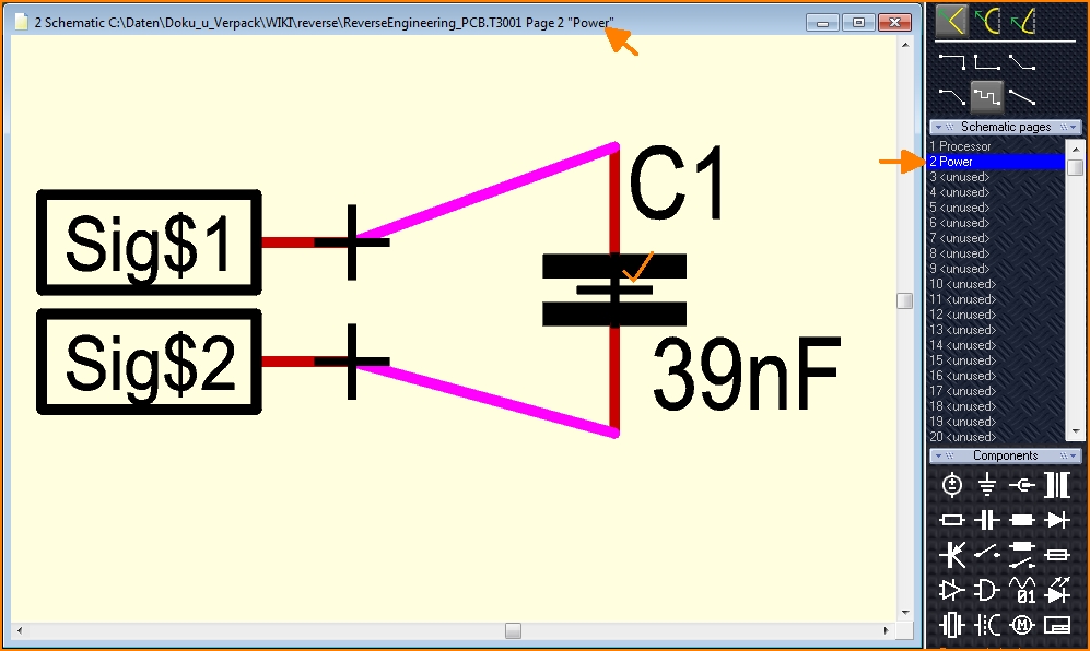
Image: Next schematic page: Reference symbols lead the two signals to the component.
Here again the signals need to be connected according to the purple air wires. The same procedure as shown above.
Finish
Finally, when all the layout work is done, cut off the corners of the board outline (layer 23) according to the template, if you have not already done so. To do this, simply highlight a vertical edge line of the board outline. Click a black touchpad at the tip of a line by [M2]. A context menu opens. It gives option to "Miter the corner". Just entering the measurements of the cut will do it. Then delete the original image from layers zero or layer 14. Decide if you want to create a ground plane now (maybe independently from the image).
By the way: You can also underlay images of inner layers. To do this, you would have to have X-ray the original board to create images representing the conditions on inner layers. This might sound unusual, but it's simple to do.
In edition "design station"...
The edition design station, offers a further, different solution focusing on "Reverse Engineering". It works since version 15 and still does beside the above mentioned:
The company Diagnosys offers a printed circuit board diagnostic system called "Pin Point", which generates the corresponding net list by pin point scanning. TARGET 3001! reduces the complexity of the netlist by a heuristic approach. Components and signals are clearly allocated to several schematic pages using a Simulated Annealing algorithm. This makes it very easy to create a new board layout from the old one. This feature is only available in edition "design station".
Delayering a six-fold multilayer board
The following images show the individual layers of a 6-fold multilayer, ready for reverse engineering.
