Double sided layout
The more complex a project gets the more difficult is it to route all tracks on one single copper layer without overlapping. Now you will have to use the copper top side (populating side, part side) for routing tracks. For leading tracks from one side to another one uses vias (a via is a plated through hole). During the process of placing tracks please press the full stop key [.] upon your keyboard to change the copper layer. A via is created and the track continues on the other copper side. Now you have a design double sided plated through (DSPth).
Settings for a double sided PCB in TARGET 3001!:
- [F3] for getting to the PCB view
- [Strg] + [l] for opening the dialog "PCB-Layers"
- choose "Standard layer set"
- double sided
- Set the layer function of layer 02 to copper bottom, and the layer function of layer 16 to copper top. When using/setting the auto router dialog please permit routing upon these two layers. Define a preferred direction of routing (orthogonal to each other).

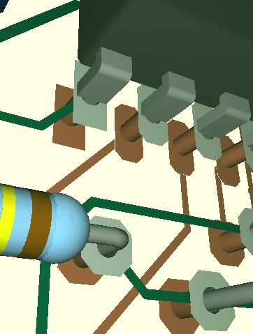
Image: 3D-view of a double sided layout. The FR4 core of the board is faded out.
The component leads stick in a husk having landmarks top and bottom.
- Green tracks: Copper top, while covered with solderstop agens.
- Tracks in copper color: Copper bottom, view from the top. Viewed from the bottom they would be green as well.

