Single sided layout
A layout is "Single sided" if all signal leading copper tracks run on only one side of a board. Mostly the soldering side is chosen (in TARGET : layer 2, copper bottom).
An example for a single sided layout please find in the TARGET 3001! Crash course.
By default the construction of a doublesided layout is set in TARGET 3001!. You need to switch over to a single sided construction actively. This can happen at the very beginning of your project:
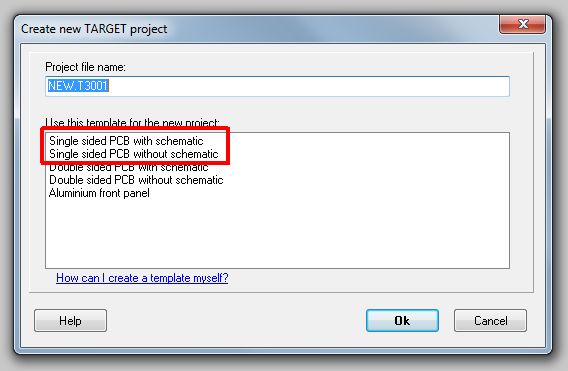
Image: Decision for the layout construction of your board at the beginning.
Or while the project already had been started:
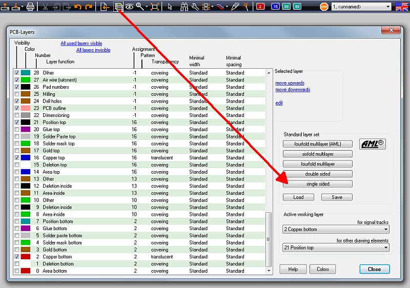
Image: Decision for the layout construction of your board while designing.
What happens when pressing the "single sided" button? The function of layer 16, copper top, will be set to "Other". At the same time this layer gets blocked for all auto router activities. Alternatively get to the above image by pressing functional key [F3] for reaching the PCB view and pressing [Ctrl]+[L] for setting layers.
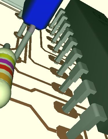
Image: 3D view of a single sided layout.
The collar of an IC lead shows where copper top would appear in a double sided layout. Here we only see copper bottom. the body of the board itself (FR4 material) is faded out as well. The soldering pads need to be defined on Layer 2, copper bottom, not on layer 100 (=through all layers). Thus there is no inner galvanizing of the drill holes. This will reduce the stability of the soldered leads a bit.
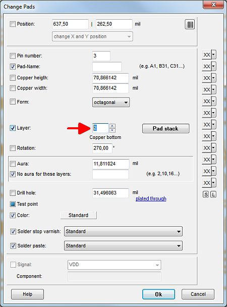
Image: Soldering pads in a single sided design on layer 2.
For autorouter use:
Press [F9] in the PCB view to start the autorouter (F9 in schematic view starts the simulation). Click on the upper TAB "Algorithm" and set 3 Passes (Disentangling) and 2 Passes (Optimization). The slider "Routing against the preferred routing of a layer" set 3/4 to "forbidden". The slider "Use of vias" leave in the middle between "forbidden" and "doesn't matter". Click on TAB "Route layers". Click on button "Default". Block the upper layer for routing of all layers. Only copper bottom must be allowed for routing without a preferred routing direction. Press the [Start]-button.
Minimum track width: in TAB Signals either select individual ones e.g. GND + VDD or all. By a doubleclick on a signal in the schematic set its minimum track width (for the routing in PCB mode) by the use of the Properties button let's say to 1 mm.
Also see: Double sided layout
