Signal polygon
For the handling of polygons with a signal in V17, V16, V15... please have a look here: Freehand groundplane
General
From TARGET V18 onwards, a ground plane is treated as a signal polygon and can be equipped with individual attributes. This means, every ground plane is a signal polygon, but not all signal polygons are automatically ground planes. Any number of signal polygons can be created on one copper side. A copper element is considered connected when its center touches the filled polygon.
You can reach this mode to draw a signal polygon:
- by keyboard key [6],
- by menu item "6 Draw ground polygon" in menu "Elements"
- by icon
 among the drawing functions
![]()
Icon to be found in the layout view among the drawing functions
Construction of a ground plane in TARGET
A ground plane (for example for the signal GND) in TARGET must be imagined as a set of three planes:
- On the area layer, the contour of the ground plane is displayed as a filled polygon
- On the deletion layer the auras (= the safety distances to the non-GND signals) which pass through the ground plane are shown
- On the copper-layer the conductive tracks and all other conductive elements are .
Tracks which do not carry the signal of the ground potential do not belong to the ground. They get an aura, a safety spacing, which is shown on the deletion layer. So they get separated from the ground. Tracks that belong to the ground plane do not have an aura. They get embedded to the ground plane and thus connect the ground plane to GND.
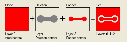
Setup of a ground plane in TARGET
At the very end of the layout work the ground plane contour of the area layer should be shifted to the copper layer together with the auras of the deletion layer. We say the signal polygon is filled or the computation in the copper layer is executed. So there are
two states of a ground plane: filled, computed and not filled, not computed.
The advantage of the not computed state (a graphical area separation) is that any change to the ground plane is immediately visible on the screen without any loss of time. Therefore it is best to fill the ground plane only at the very end, when you go for production. Otherwise you maybe pour your set in copper too early and further layout work will be ponderous a bit. However, you can turn bsck a filled ground plane into the not computed state easily.
Old polygons found
If you open a project which had been created by a version V18 or older, the following dialog will appear:
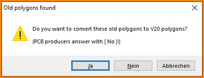
Image: The dialog "Old polygons found"
What's behind it?
If you have created a project with a version V18 or older, the conversion of polygons might cause minor changes to the polygon surfaces (roundings, etc). The printed circuit board would then look slightly different than it appeared earlier. Therefore, PCB manufacturers should not carry out the conversion. However, the normal user should convert old polygons to new ones. The new polygons are easier to handle and more flexible than the old ones. It is preferable to compute the new polygon filling at the end of the design process and leave it in a primitive state, see the option "Compute filling" at the bottom of the following dialog. Then one can fade in/out each of the layers involved separately ("copper", "deletion", and "area") the same as in earlier versions. The functions "Check project" as well as the creation of Gerber data will fill the areas later anyway.
Use the entire PCB area

Image: Use the entire PCB area for a ground plane
Create a partial ground plane area like a polygon
If not the whole area of your PCB is to be used as ground plane but only a smaller area, this can be defined as signal polygon. Select the signal polygon function with the keyboard key [6] and set the corner points of the polygon with M1. In the last polygon segment, press [Return] or M2 to end the polygon course exactly at the starting point. The dialog for editing the signal polygon opens immediately:
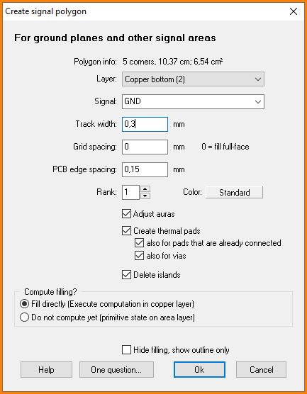
The dialog for signal polygon edition
Polygon Info
Nearly self explanatory: Shows the number of corners, the perimeter and the surface area are either metric or imperial, depending on the unit set. The values cannot be edited here.
Layer
A polygon with signal assignment can only be created on a copper layer. The copper layers used in your project can be selected from the drop down list. Select the copper layer upon which your polygon later shall appear (copper bottom, copper top, copper inside).
Signal
Select the signal to be assigned to the polygon. At this point you can only assign one signal to one polygon. Creating a Star shaped ground is a separate topic. Please have a look there.
Track width
In easy words track width is the thickness of the pen which you use to fill the polygon with color. Sounds a bit childish but in respect to the production technique it is the best way to compare. In Gerber a photo pen follows the lines on a photosensitive board with an aperture according to the track width. The sharper the tip of the pen, the more filigree structures can be built. Discuss the smallest value with your PCB-house. Here in Europe the minimum value of 0.15 mm is common.
The following picture shows the polygon with a little notch see arrow. The reason is a track width set too wide. The pen can not go through this bottle neck.
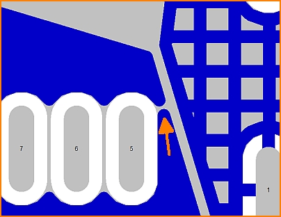
Track width too big to close the area at this spot.
Referring to the track width set here the DesignRuleCheck later checks whether the minimum track width od a connection is fulfilled. The track width must also be seen in combination with the "Grid spacing". A gridded ground plane in consists of a net-structure made of orthogonal intersecting lines. The width of this lines you also define here. You can only enter one value for the track width here. The net structure (= ground plane in lines) always has a square mesh structure.
Grid spacing
A ground plane in lines offers production advantages in galvanization and also is preferable in respect to electromagnetic performance of the signal. In addition to the track width you can define the distance of the mesh, the grid spacing.
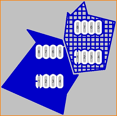
Copper top: Ground plane in lines (to the right). Track width: 0.3mm, Grid spacing: 0.5mm
NOTE: If the grid spacing gets too wide, the polygon will not be able to convey the signal any more. The limit is:
Grid spacing > Minimum Drill hole diameter + 2 x Width of the rest copper concerning pads
If you use the "Check project" routine or if you "Compute Air Wires (Ratsnest)" such a widely spaced polygon grid can not convey the signal which should run through it. So there will remain an air wire and the soldering pads in question need to be connected by a signal track manually.
The following message could appear when using the "Check project routine"
"Signal-Polygon too chunky: GND on layer 2..."
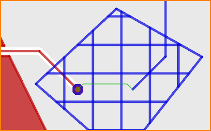
Copper top: The ground plane is gridded too wide. Please use a smaller grid.
PCB edge spacing
It is helpful to have a little spacing between ground plane and cutting edge of the PCB. It can avoid a short circuit by just touching the board by any other object. Also a crosstalk of the signal can be avoided. Define here how far you put back the edge of the ground plane from the edge of the board. Cutting edge of the board is middle of the PCB outline.
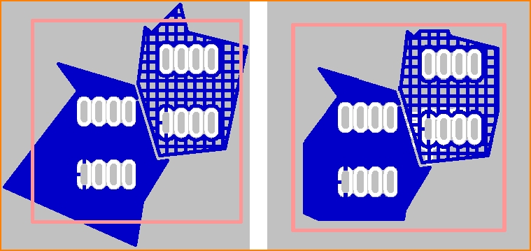
Distance to the edge: left without, right with "stand back" from the edge of the board. In the image to the right the left polygon shows a PCB edge spacing of 0.8mm, the one right beside shows a spacing to the edge of 0.4mm.
Rank
Polygons can overlap, they even can interlace - sure they never should touch each other. Which of the polygons should dominate the other (taking away some of the others shape) can be defined by its rank. The higher the cipher of the rank of a polygon is, the more dominant it is. A polygon with rank 2 dominates a polygon having only rank 1. This means the one with rank 2 takes away the overlapping from the one with rank 1 and so on. There are 99 ranks possible.
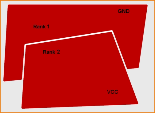
Copper bottom: Interlacing polygons with different signals and different ranks.
The distance between the two surfaces is determined by the value of the "Spacing between single signals", see default entry in the "Check project" dialog. Unless the individual entry for the "Minimum track spacing" of one of the signals (or their signal classes) would be set larger. Then this value would be used. So the higher value of both will be used to determine the gap.
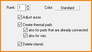
Adjust auras
If you create a new signal polygon, the auras of the tracks, vias and pads touching the polygon or being inside the polygon will be adapted. If you later edit the auras manually, they will not be adjusted automatically when you refill the polygon unless you check the "Adjust auras" box. The following will happen:
- a different-signal pad/via gets isolated
- a same-signal pad gets a thermal
- solder pads without pad number get a thermal too
- a same-signal via will be completely embedded to the plane
Afterwards you can manually change the auras of the individual soldering pads and vias. TARGET will not propose to adjust the auras when recalculating the polygon. If you want to embed a pad completely, you can set its aura to zero later or use the field "No aura for these layers:" and list the corresponding copper layer(s). Then let the area (s) be refilled, i. e. the dialog "Edit signal polygon" needs to be opened again and the option "Fill directly (Execute computation in copper layer)" needs to be ticked. Vias never get automatic heat sinks. In general vias are always connected over their entire surface (= embedded). If the user later adds an aura to the via on the ground plane layer, it remains isolated in this ground plane, i. e. unconnected.
Create thermal pads
The soldering pad of a component lead having the same signal as the ground polygon, e. g. GND, should be fully embedded in order to connect as best as possible. However, too much heat would dissipate into the ground plane too quickly during soldering, so that the solder agens would not bond well with the copper. Better create a thermal pad. A thermal pad (heat sink, thermal) is a soldering pad which is surrounded by a safety spacing (aura) but connected to the ground plane by small bars only. This prevents the heat energy from dissipating into the plane too quickly when getting soldered. These automatic bars are cross-shaped to the pad.
also for pads that are already connected
If the sub-option "also for pads that are already connected" is selected (default), then those soldering pads will get 4 ligaments (ridges) if possible, which were already connected to tracks manually or by the use of the autorouter. If this box is unchecked, no ligaments (ridges) will be created for all soldering pads from which a manually routed track starts.
The width of these automatic thermal ligaments from V20.5.0.17 is:
- for drilled pads max 2/3 of the drill hole
- for SMDs max 2/3 of the thin side
- as least the filling width of the polygon
- at most the double of the filling width of the polygon
The width of the automatic thermal ligaments was before:
- at least as wide as the line width of the polygon (except for very narrow SMD pads, finepitch)
- maximum double the width of the fill lines of the polygon
- maximum width as the smaller side of the pad (pad height, pad width)
- maximum as wide as 2/3 of the larger side of the pad (pad height, pad width)
You can connect these pads with wider tracks manually. Polygonal pads are not automatically connected with ligaments (=not automatically made thermals).
Why do those ligaments in thermal pads lead into empty space sometimes?
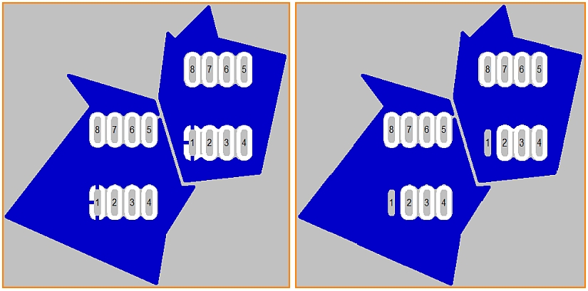
The pads numbered 1 of the two components being located to two polygons. Left with thermal pads, right without - thus embedded completely to the plane.
also for vias
TARGET will completely embed a via in the ground plane if it carries the same ground potential. Since a via is normally not soldered, there is no reason why this should not be the case. If you still want to equip your vias like a heat sink with aura and ligaments (ridges), you can check this box.
Suppress ligaments in thermals
If you don't like the ligaments, double-click the via and untick the ligaments-box in the dialog (underneath the PadStack button). Now you could set them manually as a simple copper rectangle furnished with the same signal.
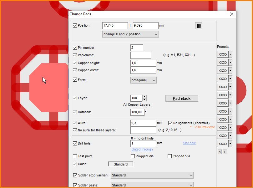
Image: Option (untick box) to actively suppress the creation of ligaments if the object comes out as a thermal.
Delete islands
A not connected piece of a signal polygon is called "island" or "orphan". They dont have any purpose and often make trouble. So they should be removed. TARGET does this automatically if you tick the box. A ground plane gets connected by a pad of a component, a via having an aura of 0 upon this layer or a piece of track running through the polygon plane and having aura =0. Always the signal name (the signal) must be identical.
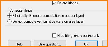
Compute filling
Filling here means something like "copper pour". It is when you merge the signal track structures and the ground area on the copper layer. TARGET then renders the complete structure of "Copper top" or "Copper bottom" (or "Copper inside" if you have) including the ground plane. You can do it instantly ("Fill directly") by confirming the dialog or you can leave the construction in an intermediate state ("Do not compute yet") so that the signal polygon of the ground plane is defined like a primitive. It is kept in waiting position to be handled separately on the "Area"-layer. So the ground plane still can be adapted, moved and trated as you please.
Fill directly (Execute computation in copper layer)
The polygon immediately gets created wit all interactions to all other elements upon the copper layer. It is displayed the way ist will be produced at the end. Any change in design requires the complete computation (rendering). This process can take some seconds in bigger projects. Therefore it might be better to use the option: "Do not compute yet (primitive state on area layer)" see below.
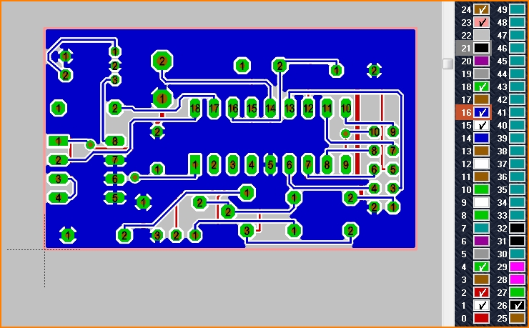
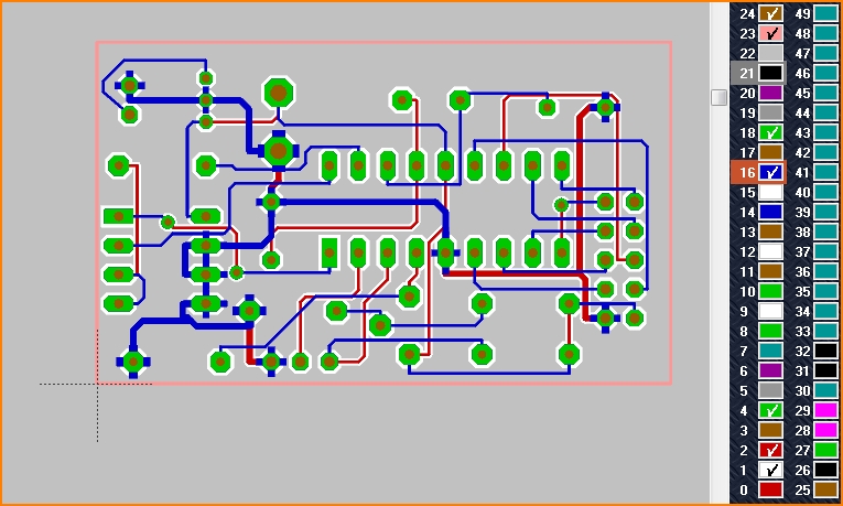
Image: Example of a double sided Layout, ground plane on copper top, filled directly.
Do not compute yet (primitive state on area layer)
If you select this item, the ground plane at first is built up three-layered:
- Its shape on layer "Area", it is the primitive of the ground plane
- The auras of all signals on layer "Deletion", i. e. the spacings of all signals giving clearance to the ground potential (s).
- The tracks on layer "Copper". All signal tracks including the ground signal (s) are displayed here.
Example:
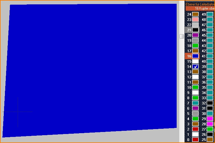
Image: The ground plane as a priitive created by keyboard key [6] Draw signal polygon. It is displayed on layer "14, Area top".
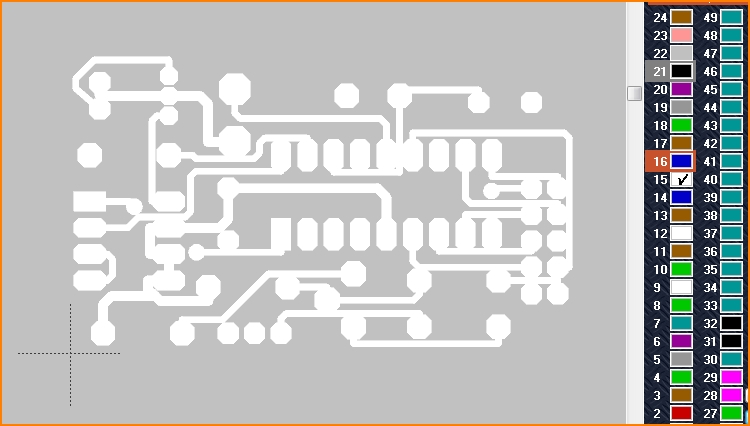
Image: The aura of each of the signals is displayed on layer "15, Deletion top".
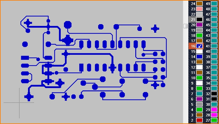
Image: DThe copper tracks on layer "16, Copper top"
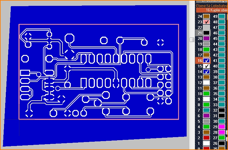
Image: All three layers Copper, Deletion and Area are faded in, in addition layer "23, PCB Outline" (light red). The state still is "Not yet computed", because the three layers are still separate which means not yet "poured into copper". Ticking the boxes to the right each fades them in, unticking fades them out.
Unfill an already filled (computed) ground plane
Retrieve an already computed filled ground plane to the three levels copper, deletion and area by selecting the entry "Do not fill all polygons" in menu Actions/Ground planes. Now you can show, hide and edit the groundplane separately.
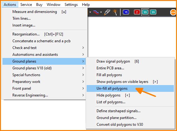
Image: The ground plane is a triplet again
Hide filling, show outline only
This is for a better overview and easier grip of elements within the ground plane.
Show or hide polygons upon visible layers
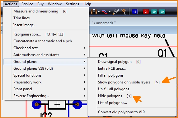
Image: Show and hide polygons
The key [>] fills polygons on visible layers. So they get visible, if area- and deletion layers before had been faded out. Apart from this they are just calculated new.
The key [<] un- fills all polygons, shifts them to the area layer and fades out all area- and deletion layers. The polygons get faded out so to speak. Only the ligaments of thermal pads remain.
The key [-] un-fills all polygons, moves them to the area layer and ,akes all area and deletion layers visible. The polygons remain visible, but are in a non-calculated state.
Create a keep out area
A keep out is an "area within a copper area" free of copper. Draw it in any shape (rectangle, trinagle, circle, normal polygon) into the deletion layer of the respective copper side. Maybe the "Fill directly" command for the signal polygon has to be executed again to have the keep out take effect.
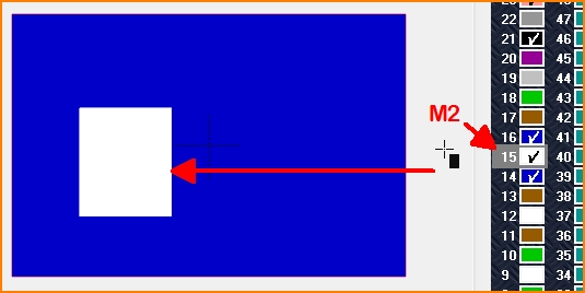
Image: Draw a keep out to the deletion layer: Select drawing mode, right click (M2) the desired layer in teh sidebar, draw the keep out area. (alias keepout, keep-out)
List of polygons
This is an item in layout menu "Actions/Ground planes". Several signal polygons in a project are clearly displayed in a list. All relevant properties of the signal polygons are visible at a glance.
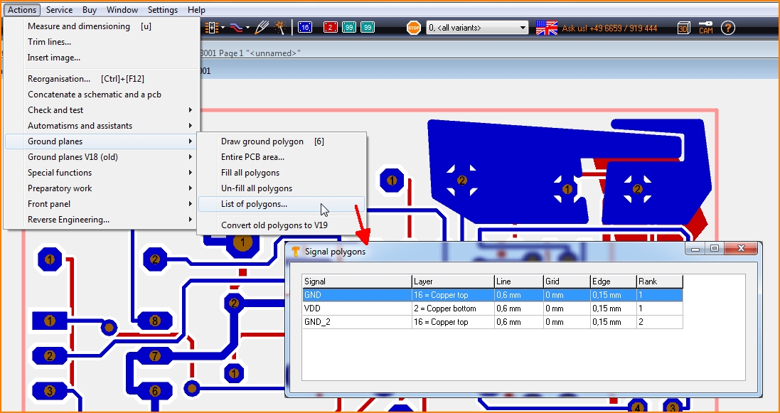
Image: List of signal polygons with different properties in one project: Signal name, layer to appear on, line width of filling (=track width), grid spacing, distance to PCB edge and rank.
Rank 2 dominates rank 1, rank 3 dominates rank 2 and/or 1, and so on. When overlapping, the polygon with the higher rank digit takes away something from the polygon with the smaller rank digit. See "Copper top" (blue): The polygon on the left has rank digit 2, which is higher than the polygon on the right, having only rank digit 1. The red polygon has also rank digit 1, but this is irrelevant in this construction, as it is located on "Copper bottom".
Double-clicking on the first line of the list displays the following screen:
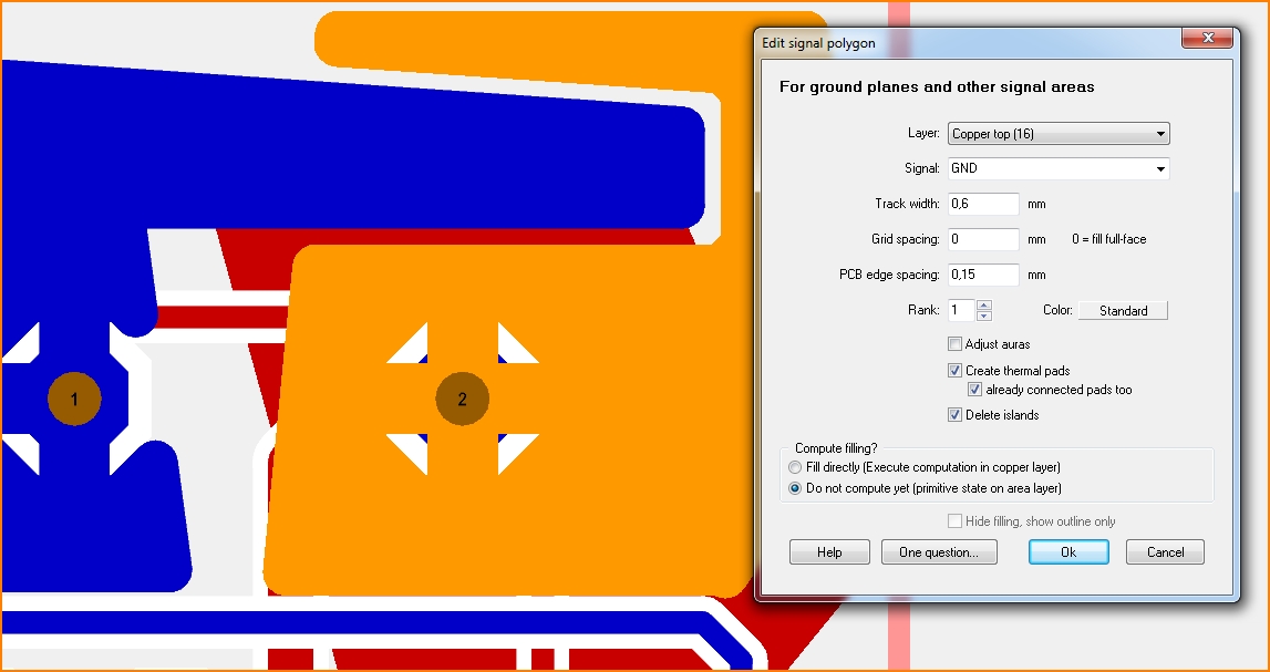
Image: Clicking M11 to a list entry zooms to the respective signal polygon and marks it. At the same time its dialog: "Edit signal polygon" opens for inspection/edition.
Text in a ground plane
Please have a look here:
Text in ground plane
Delete groundplane
Highlight groundplane by mouseclick M1 and delete it by pressing the [Del] key.
Attention when making changes after "filling"!
When you render the filling of a ground plane (execute the computation in copper layer, "fill"), this is done exactly representing the conditions that apply at the time of rendering. If you make changes to elements having an aura afterwards or change deletions or other parameters that will influence the area, then the area will have the wrong shape prior to the next rendering! Therefore, when checking the project or calculating the air wires and with each new output, the area always will be recalculated so that all current conditions are taken into account.
Unfortunately, the project can be saved in this inconsistent state before recalculation. When outputting data for manufacturing, the correct recalculation of all surfaces is then carried out, which can lead to differences. To make sure that the PCB looks on the screen as it will be produced, always run "Check Project" in menu "Actions/Check and test" as the last step before ordering.
alias: freehand groundplane, customized ground, copper pour, copper fill
