Component Interchange Format (CXF)
Preface
The Component Interchange Format (CXF) is a new smart ASCII format. Every electronic component used on PCBs can be described using this format. It is easy to understand and by this means it easily can be adopted/used by anyone having the need of interchanging CAD data of electronic device. CAD data means a schematic symbol and a footprint pattern.
A CXF can contain several components. A component can have several schematic symbols (at least one) and normally one package. A resistor for example has one symbol and one package. A logic IC can have several symbols (gates) while using only one package.
A symbol and a package consist of several graphic primitives like lines, texts, rectangles and pins in the symbols and pads in the package. Every primitive is written into one text line and starts with a specific identifier. Several predefined fields may follow. Every primitive can also have several user defined properties, each property written in an own line. Properties do not contain CR/LFs but can be extraordinarily long (100000+ Bytes). The possibility of user defined properties for every primitive makes the format future proof.

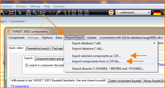
Image 1: How to import or export CXF data to or from the TARGET component data base.
Following this link you will find a short CXF file using some of the different primitives.
The Syntax
The fields on each line are separated by TABs. Therefore the field contents must not contain TABs. If a field value matches it's default content, then it can be omitted.
COMPONENT    NAME=USBUF01W6    VALUE=    PREFIX=IC    SYMBOLS=1    PACKAGE=13    PROPERTIES=7

COMPONENT       identifier
NAME=USBUF01W6     search-name of the component
VALUE=     value of the component, if available
PREFIX=IC    prefix for the component name (IC8, R12)
SYMBOLS=1    how many symbols will follow? (Default=0)
PACKAGE=13    how many graphical primitives has the package? Inclunding the handle cross (Default=0)
PROPERTIES=7     how many user-defined property lines will follow? (Default=0)
LAST_MODIFIED_BY=K11970
LAST_MODIFIED=2008.12.30 18:44:16
...
These 2 lines are the first two of the 7 user-defined properties as announced in the COMPONENT line (header). Properties are always first, then the package primitives follow and then the schematic symbols.
PACKAGE    NAME=SOT323-6L    X1=0    Y1=0    LAYER=4

PACKAGE    identifier
NAME=SOT323-6L    name of the proposed package
X1=0    position of the package grip (handle)
Y1=0    all coordinates are in nm = 1/1000000 mm = 1/1000 µm. We use the normal cartesian coordinate system with the origin the in middle. Integer format.
LAYER=4    denotes the layer function. Layer functions are described later
PROPERTIES=0     how many user-defined property lines follow? (Default=0)
PAD    XM=-650000    YM=-950000    WIDTH=350000    HEIGHT=1000000    LAYER=2    PINNUMBER=1

PAD    identifier
XM=-650000    YM=-950000    center coordinates [nm], default = 0
WIDTH=350000    pad width [nm], default = 0
HEIGHT=1000000    pad height [nm], default = 0
LAYER=2    on copper top only, SMD pad. 0 for symbols elements. Default = 0
PINNUMBER=1    number for assignment PIN to PAD, 0 = no pin for that pad = default
FORM=3     pad form, 0=round , 1=octagonal, 2=rectangular, 3=oblong (default), 4=polygonal (see POLY_PAD property below)
ROUNDED=0    rounding [%]. Integer. For rectangular pad form only
ROTATION=0    all angles 0 .. 360, floating point value, max 4. decimal digits, [,] or [.] as decimal separator possible.
0=right=default, 90=top, 180=left, 270=bottom
DRILL=800000    drill hole [nm]. No drill = 0 = default
LONG=1200000    oblong drill hole length [nm]. Normal drill hole = 0 = default
PADNAME=C23    optional for alphanumeric pad names
STOP=0    solder stop varnish: 0=standard, 1=pad completly free, 2=only drill hole free, 3=pad completely covered
PASTE=0    solder paste: 0=standard, 1=pad covered with paste, 2=no paste
PROPERTIES=0     how many user-defined property lines follow? (Default=0)
POLY_PAD=-1000000,-700000;-1000000,700000;100000,1800000;1000000,700000;1000000,-700000 polygon coords [nm]. Property. No self-intersection. Self-touching ok for inner holes
LINE    X1=-1100000    Y1=675000    X2=1100000    Y2=675000    WIDTH=300000    LAYER=4

LINE    identifier
X1=-1100000    Y1=675000    coordinates of start point [nm], default = 0
X2=1100000    Y2=675000    coordinates of end point [nm], default = 0
WIDTH=300000    line width [nm], default = 0
LAYER=4    see above
DASHED=0    0=solid (default), 1=dotted, 2=dashed, 3=dashdot, 4=dashdotdot
ROUNDED=YES    round line caps, default = YES
PROPERTIES=0     how many user-defined property lines follow? (Default=0)
TEXT    CONTENT=!BAUTEIL    X1=-1250000    Y1=2950000    WIDTH=1500000    HEIGHT=1500000    LAYER=4    WEIGHT=10    FUNCTION=1

TEXT    identifier
CONTENT=!BAUTEIL    current content, special, if FUNCTION is not 0
X1=-1250000    Y1=2950000    coordinates of foot point [nm], default = 0. Text is displayed in math. quadrant No 1 relative from that foot point
WIDTH=1500000    character width [nm], default = 0
HEIGHT=1500000    character height [nm], default = 0
LAYER=4    see above
WEIGHT=10    weight of the font in %
ITALIC=YES    italic font, if available
RIGHT=YES    align text right
FUNCTION=1    denotes the text function. Text function are described later
HIDE=NO    text is invisible (for invisible pin names)
ROTATION    see above
DYN=YES    text is always readable from below or from right (default).
MIRR=NO    text is mirrored
GERMAN=Hallo    for documentation in German language
ENGLISH=Hello    for documentation in English language
FRENCH    for documentation in French language
PROPERTIES=0     how many user-defined property lines follow? (Default=0)
SYMBOL    X1=0    Y1=0    LAYER=101    SUFFIX=a    NUMBER=1    ELEMENTS=12

SYMBOL    identifier
X1=0    Y1=0    coordinates of grip handle [nm], default = 0
LAYER=101    see above
SUFFIX=a    suffix for the symbol name, e.g. IC1a
NUMBER=1    number of the symbol within the component normally 1, 2, 3, ...
ELEMENTS=12    how many graphical primitives are following? Caution: PROPERITES might come first! Caution: The PIN names do not count as own primitives in this case; see next section
INSERT=YES    this symbol is always directly imported (default = YES)
SWAP=0    this symbol can be exchanged with symbols of the same component having the same swap level, default = 0 = no swap
PROPERTIES=0     how many user-defined property lines follow? (Default=0)
PIN    X1=-11430000    Y1=2540000    PINNUMBER=1    PINNAME=YES    LENGTH=2540000    WIDTH=300000    LAYER=1
TEXT    CONTENT=D1    X1=-8390000    Y1=1790000    WIDTH=800000    HEIGHT=1500000    LAYER=1    WEIGHT=13    FUNCTION=5

PIN    identifier
X1=-11430000    Y1=2540000    coordinates of start point [nm], default = 0
PINNUMBER=1    number for assignment PAD to PIN, a number > 0 is necessary
PINNAME=YES    this PIN primitive line is followed by a TEXT primitive giving the pin name. This following pin name is a sub-primitive of the PIN and does not count for the SYMBOL
LENGTH=2540000    pin length [nm], default = 0
WIDTH=300000    pin line width [nm], default = 0
LAYER=1    see above
PADNAME=C12    optional for alphanumeric pad names
ROTATION=0    see above
FUNCTION=6    electrical function of the pin, default = 6 = passive
SWAP=0    this pin can be exchanged with another pin in this symbol having the same swap level, default = 0 = no swap
INV=NO    small circle to indicate an inverted pin, default = NO
CLOCK=NO    small hook inside PCB to indicate a clock related pin, default = NO
SHOWNUMBER=YES   display the small automatic pin number besides the pin, default=YES
REF=NO   the pin is a special pin for a voltage or signal reference such as a GND designator, normally not used in a CXF, default = NO
PROPERTIES=0     how many user-defined property lines follow? (Default=0)
The above are primitives which had been used in the small sample.
Further primitives
TRIANGLE    identifier
X1=0    Y1=0    filled triangle coordinates of first point [nm], default = 0
X2=0    Y2=0    coordinates of second point [nm], default = 0
X3=0    Y3=0    coordinates of third point [nm], default = 0
LAYER=0    see above
PROPERTIES=0     how many user-defined property lines follow? (Default=0)
RECTANGLE    identifier
X1=0    Y1=0    filled rectangle coordinates of left-bottom point [nm], default = 0
WIDTH=0    rectangle width [nm], default = 0
HEIGHT=0    rectangle height [nm], default = 0
ROTATION=0    see above
LAYER=0    see above
PROPERTIES=0     how many user-defined property lines follow? (Default=0)
ARC    identifier
XM=0    YM=0    coordinates of the arc center point [nm], default = 0
X1=0    Y1=0    coordinates of start point [nm], default = 0
X2=0    Y2=0    coordinates of end point [nm], default = 0
RADIUS=0    radius of the arc [nm], default = 0
WIDTH=0    line width [nm], default = 0
START=0    start angle (see ROTATION above)
END=0    end angle, full circle with START=0    END=360
DASHED=NO    dashed line, default=NO
ROUNDED=YES    rounded end caps, default=YES
LAYER=0    see above
PROPERTIES=0     how many user-defined property lines follow? (Default=0)
DISK    identifier
XM=0    YM=0    coordinates of the filled disk center point [nm], default = 0
RADIUS=0    radius of the disk [nm], default = 0
LAYER=0    see above
PROPERTIES=0     how many user-defined property lines follow? (Default=0)
FIDUCIAL    identifier
XM=0    YM=0    coordinates of the fiducial center point [nm], default = 0
ROTATION=0    see above
RADIUS=0    radius of the fiducial [nm], default = 0
WIDTH=0    line width [nm], default = 0
FORM=3    form of the fiducial: 0=target, 1=arrow, 2=two_quarters, 3=disk=default; also see here.
LAYER=0    see above
PROPERTIES=0     how many user-defined property lines follow? (Default=0)
SPLINE    identifier
X1=0    Y1=0    coordinates of spline start point [nm], default = 0
X2=0    Y2=0    coordinates of spline end point [nm], default = 0
XA=0    YA=0    coordinates of spline attraction point [nm], default = 0
WIDTH=0    line width [nm], default = 0
LAYER=0    see above
PROPERTIES=0     how many user-defined property lines follow? (Default=0)
Normally the next two do not belong to a CXF. But they might appear:
ERROR    identifier
XM=0    YM=0    coordinates of the DRC error marker's center point [nm], default = 0
RADIUS=0    radius of the error marker [nm], default = 0
TEXT=    textual explanation of the error, default =
LAYER=0    see above
PROPERTIES=0     how many user-defined property lines follow? (Default=0)
SIGNAL    identifier
NAME=    name of the signal, default=
PROPERTIES=0     how many user-defined property lines follow? (Default=0)
Finally the missing field descriptions:
Layer functions
TARGET has up to 100 layers. Caution: The LAYER token in the CXFs does not contain the layer number but the layer-function number. 4 means "Position print top". TARGET does not distinguish between position print ans silkscreen. Packages are drawn for mounting on the PCB's top side. Thus SMD pads use layer function 2 (=Copper top) and THT pads use layer function 100 (=appears on all copper layers). Here is a list with all layer function numbers:
0=Copper bottom
1=Copper inside
2=Copper top
3=Position print bottom
4=Position print top
5=Deletion bottom
6=Deletion inside
7=Deletion top
8=Area bottom
9=Area inside
10=Area top
11=Solder mask bottom
12=Solder mask top
13=Drill holes
14=Solder paste bottom
15=Solder Paste top
16=Gold bottom
17=Gold top
18=Glue bottom
19=Glue top
20=Dimensioning
21=PCB outline
22=Milling
23=Pad numbers
24=Air wire (ratsnest)
25=Signal names
26=Route prohibition (Copper bottom)
27=Route prohibition (Copper top)
28=Route prohibition (Copper inside)
29=Blind via prohibition top
30=Blind via prohibition bottom
31=Buried via prohibition
32=Component names top
33=Component values top
34=Component names bottom
35=Component values bottom
36=Frontpanel (milling)
37=Frontpanel (documentation)
38=Frontpanel (lettering)
39=Position inside bottom (AML)
40=Position inside top (AML)
41=Separation into single PCBs
100=appears on all copper layers
Text functions
0=Normal text
1=Component name (IC17, R3, ...)
2=Component value (10k, 20µF, 7805, NE555, 2N3055)
3=Symbol name (IC17a, IC3c)
4=Signal name (seldom used in components)
5=Pin name (CLK, RES, a "|" starts and ends a overline indicating inverse function)
11=date of project last modified
12=time of project last modified
13=date of display/print
14=time of display/print
15=output scale in %, may contain '.' or ',' as decimal separator
16=project filename without extension
100=page number (schematic only)
101=user defined property of owning Signal, component or project
102=PCB variant name
103=project filename with extension
105=page name (schematic only)
Pin functions
0=NC
1=Input
2=Output
3=IO=Input/Output
4=OC=Open Collector
5=Power (power pin of a power consuming IC)
6=Passiv
7=Tristate
8=Supply (output pin of a power supply component)
9=None
10=Illegal (normally not used)
CXF allows to drag and drop components from the web to TARGET 3001!
In order to insert components from an external data base (the data base of a part manufacturer) without diversions into TARGET the clipboard is used. The external component software only needs to copy a CXF-file with a leading "$CF_TARGET_CXF" in unformatted text (CF_TEXT) to the clipboard. Immediately the component is fixed to the cursor in TARGET 3001!. The content of the clipboard is exchanged by "TARGET 3001!: Received CXF".
At the same time the component is added to the TARGET 3001! SQL data base to use it in future projects. In order to place it to the right category it might be good to ask the user where to assort it in TARGET. in this respect the external software needs to question the user about these aspects and present a selection to him. If one copies to the clipboard the pure text: "$CF_TARGET_CAT_REQ" TARGET 3001! answers the following to the clipboard:
$CF_TARGET_CAT_ANSW
$CAT Audio
$SUB Audiofilter 2
$SUB Audioverstärker 6
$SUB Radio 3
$SUB Signalgeber/Summer 8
$SUB Sonstige Audio 1
$SUB Sprache 4
$SUB Telefon 5
$CAT Diode
$SUB Brückengleichrichter 10
$SUB IR-Diode 86
...
The language of the answer depends on the TARGET edition installed: German, English or French. If the user had chosen the right category or sub-category, the part immediately can be copied to the clipboard:
$CF_TARGET_CXF
COMPONENT    NAME=CY7C1049DV33    VALUE=    PREFIX=IC    SYMBOLS=1    PACKAGE=44    PROPERTIES=6
LAST_MODIFIED_BY=K11970
LAST_MODIFIED=2010.04.27 15:30:07
COMPONENT_TYPE_ID=86
COMPONENT_FUNCTION=Digital-IC
COMPONENTTYPE=IC\Digital
LAST_MODIFIED_PACKAGE=2010.04.27 15:41:07
PACKAGE    NAME=SOJ36    X1=0    Y1=0    LAYER=4
PAD    XM=-10800000    YM=-4750000    WIDTH=500000    HEIGHT=1800000    FORM=2    LAYER=2    PINNUMBER=1
PAD    XM=-9530000    YM=-4750000    WIDTH=500000    HEIGHT=1800000    FORM=2    LAYER=2    PINNUMBER=2
...
Please note value "COMPONENT_TYPE_ID=86" in the properties, which corresponds to the selected category number. Immediately the component will be inserted to the component data base and - if a TARGET 3001! schematic window is opened - it will be fixed to the cursor to drop it to the schematic. Drag and drop also the package to the layout instantly afterwards.


