Multiple PCBs within one project
Related subject: Setting up a board as a Panel.
Within one project it is possible to divide a layout into several PCBs, or copy parts of it to have multiple PCBs in ine project, see the following example: pic.t3001
It is possible to maintain as much different layouts within one project as the size of the board allows. The maximum board size is 78.74 in² (=2.0 m²) over all.
See these two layouts within one project which you'd like to treat separately in Gerber data creation as well as in the creation of a Bill of Material:
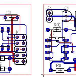
Image: Detail of two layouts within one project
First you need to use the icon ![]() to create a new layer having the function "Separation into single PCBs". Select an appropriate color and eventually a line pattern to get a somewhat translucent view.
to create a new layer having the function "Separation into single PCBs". Select an appropriate color and eventually a line pattern to get a somewhat translucent view.
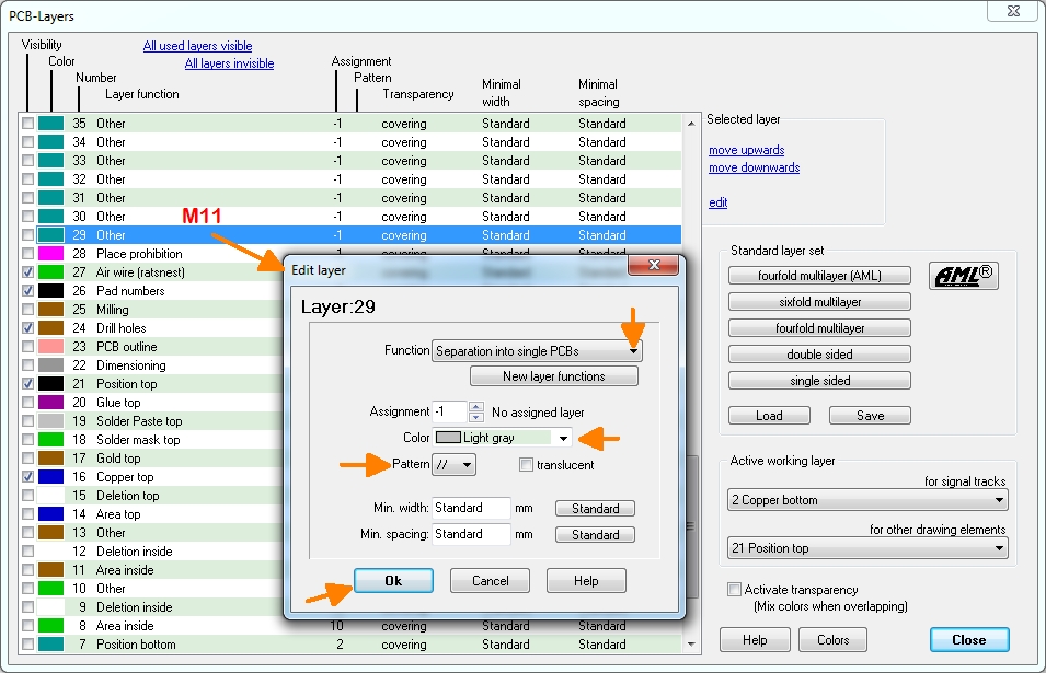
Image: Define a layer. Double click on a free layer line to open the "Edit layer" dialog. From the drop down menu select the layer function "Separation into single PCBs".
The individual PCBs now need to be covered by filled rectangles being drawn on layer: "Separation into single PCBs". In our case it's layer #29. To do so, select the "Draw filled rectangles" tool in the drawing functions and click M2 on the number of the new layer in the layer stack in the sidebar on the right. This activates a layer to draw on. This is how you always do it in TARGET: Select the drawing tool and right-click on the layer number or on the color field of the layer in the layer stack on the right to activate it. Then draw.
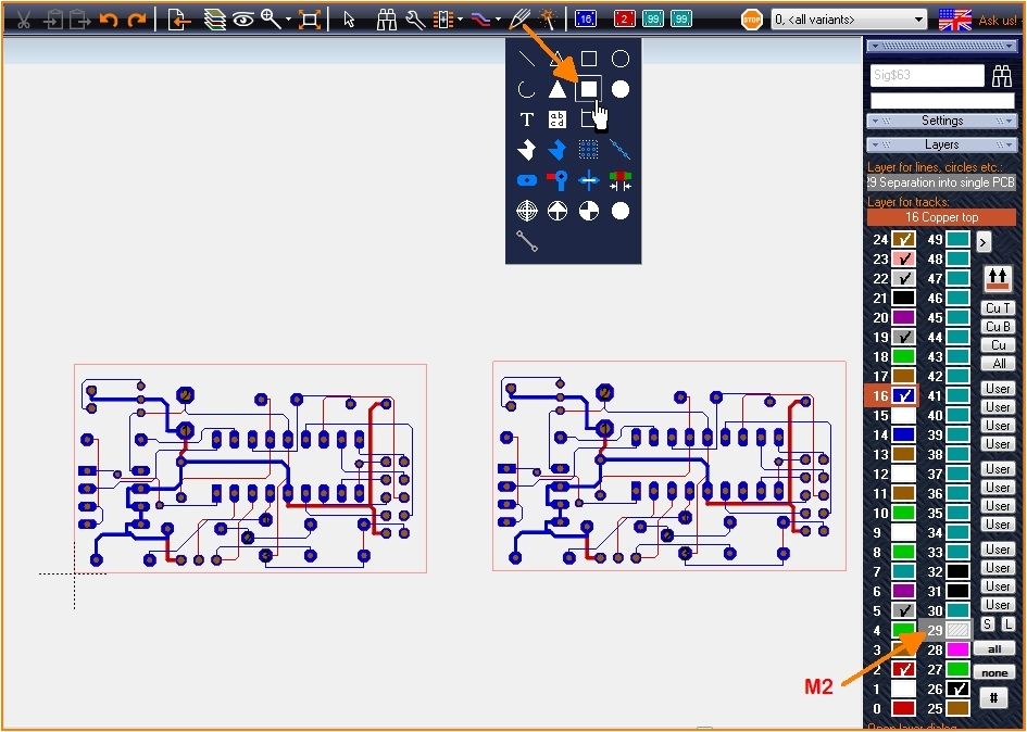
Image: Lay a filled rectangle upon layer 29 upon each separate layout.
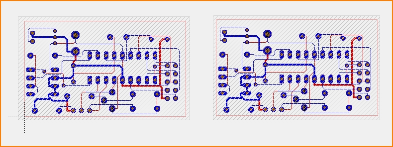
Image: That's what it might look like.
The next step is the important thing. Double click one rectangle and press the [Properties] button in the dialog. In the column "Property" type "PCB_AREA" to a free line. Right beside in the column "Value" enter an appropriate name, e.g. PCB1.
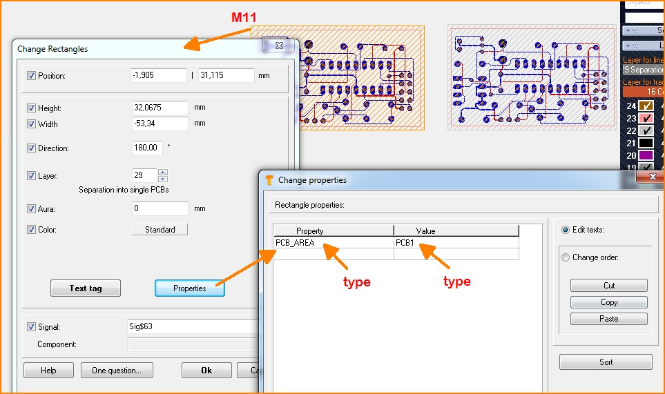
Image: Enter property and value.
Do this for all rectangles (= single PCBs). In our case you might have value PCB1 for the first and PCB2 for the second rectangle.
Both the Gerber export...
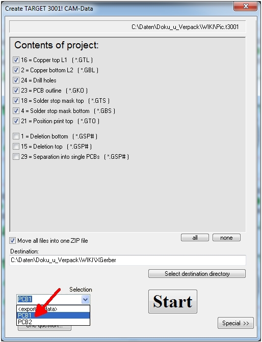
Image: XGerber and Excellon
...and the generation of the Bill of Material allow choosing one of the PCBs:
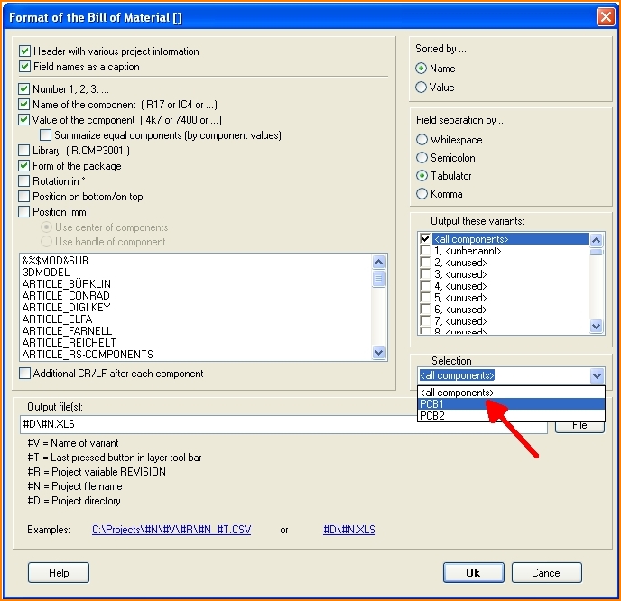
Image: Select data set for the Bill of material (BoM)]]
