Signal polygon
From version V19!
![]()
Icon to be found in the layout view among the drawing functions
General
Any filled polygon on a copper layer can be furnished with a signal. Each can be handled like a separate ground plane. It can individually be furnished with attributes. On one copper layer any number of polygons with different signals can be drawn.
You can reach this mode:
- by keyboard key [6],
- by menu item "6 Draw ground polygon" in menu "Elements"
- by icon
 among the drawing functions
What you can do
Define the corners of the polygon by M1. You can close the polygon automatically by [Return] when drawing the last segment. M2 does the same so that you end the line exactly on the starting point. Immediately the dialog for edition of the signal polygon opens.
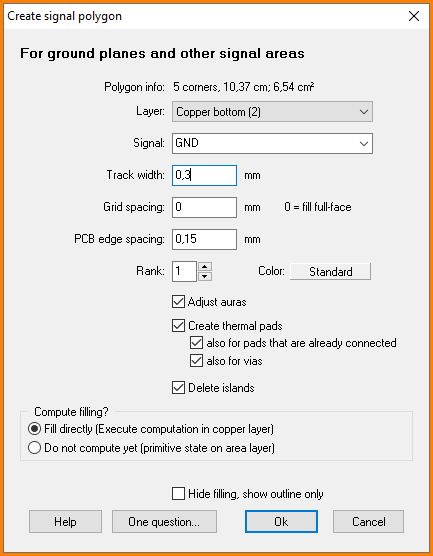
The dialog for signal polygon edition
Layer: a polygon with signal assignment can only be created on a copper layer. The copper layers used in your project can be selected from the drop down list. Select the copper layer upon which your polygon later shall appear (copper bottom, copper top, copper inside).
Signal: Select the signal to be assigned to the polygon. At this point you can only assign one signal to one polygon. Creating a Star shaped ground is a separate topic. Please have a look there.
Track width: In easy words track width is the thickness of the pen which you use to fill the polygon with color. Sounds a bit childish but in respect to the production technique it is the best way to compare. In Gerber a photo pen follows the lines on a photosensitive board with an aperture according to the track width. The sharper the tip of the pen, the more filigree structures can be built. Discuss the smallest value with your PCB-house. Here in Europe the minimum value of 0.15 mm is common.
The following picture shows the polygon with a little notch see arrow. The reason is a track width set too wide. The pen can not go through this bottle neck.
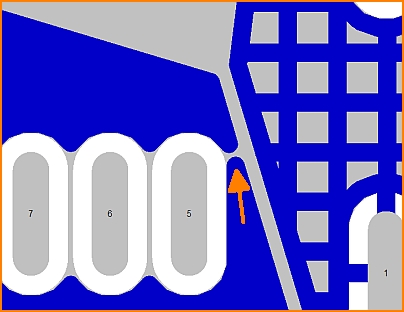
Track width too big to close the area at this spot.
Referring to the track width set here the DesignRuleCheck later checks whether the minimum track width od a connection is fulfilled. The track width must also be seen in combination with the "Grid spacing". A gridded ground plane in consists of a net-structure made of orthogonal intersecting lines. The width of this lines you also define here. You can only enter one value for the track width here. The net structure (= ground plane in lines) always has a square mesh structure.
Grid spacing: A ground plane in lines offers production advantages in galvanization and also is preferable in respect to electromegnetic performance of the signal. In addition to the track width you can define the distance of the mesh.
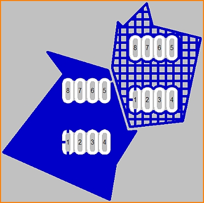
Copper top: Ground plane in lines (to the right). Track width: 0.3mm, Grid spacing: 0.5mm
PCB edge spacing: It is helpful to have a little spacing between ground plane and cutting edge of the PCB. It can avoid a short circuit by just touching the board by any other object. Also a crosstalk of the signal can be avoided. Cutting edge is middle of the PCB outline.
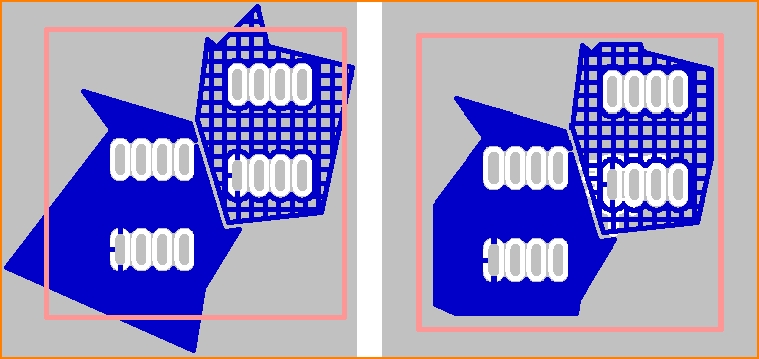
Distance to the edge: left without, right with "stand back" from the edge of the board. In the image to the right the left polygon shows a PCB edge spacing of 0.8mm, the one right beside shows a spacing to the edge of 0.4mm.
Rank: Polygons can overlap, they even can interlace - sure they never should touch each other. Which of the polygons should dominate the other (taking away some of the others shape) can be defined by its rank. The higher the cipher of the rank of a polygon is, the more dominant it is. A polygon with rank 2 dominates a polygon having only rank 1. This means the one with rank 2 takes away the overlapping from the one with rank 1 and so on. There are 99 ranks possible.
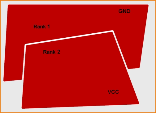
Copper bottom: Interlacing polygons with different signals and different ranks.
Create thermal pads: A thermal pad is a connecting pad which is not completely embedded to the plane but it connects only by small ligaments. It effects reduced heat dissipation into the plane. This supports good connection of solder agens and copper pad. Those ligaments can look crosswise, y-shaped or straight. Also see Thermal Pads.
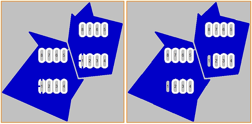
The pads numbered 1 of the two components being located to two polygons. Left with thermal pads, right without.
Delete islands: A not connected piece of a signal polygon is called an "Island". They are also called "Orphans". They dont have any purpose and mostly make trouble. So they should be removed. TARGET does this automatically if you tick the box. A ground plane gets connected by a pad of a component, A via having an aura of 0 upon this layer or a piece of track running through the polygon plane and having aura =0. Always the signal name (the signal) must be identical.
Fill directly : The polygon immediately gets created wit all interactions to all other elements. This process can take some seconds in bigger projects. Therefore you can switch it off here by unticking the box. By default the box is ticked.
alias: freehand groundplane, customized ground, copper pour, copper fill
