Check project: Difference between revisions
No edit summary |
|||
| Line 59: | Line 59: | ||
[[Image:errormarkers.png|none|Size of error markers]]<br><br> | [[Image:errormarkers.png|none|Size of error markers]]<br><br> | ||
== Ignore spacing == | |||
<br>As of V32, the check for spacing to other signals can be disabled for individual elements. This is interesting e.g. with an existing bridge in solder jumpers. If there is a standard connection in the jumper, which can be optionally scratched away later, then the check at this point always threw an error message because of a spacing violation:<br><br> | |||
[[image:IgnoreSpacingEN.jpg]]<br>Ignore spacing<br><br> | |||
A lightning bolt symbol appears in the right margin to additionally illustrate the danger of this checkbox.<br><br> | |||
== The meaning of the error messages == | == The meaning of the error messages == | ||
Revision as of 06:45, 26 July 2023
Also see Realtime design rule check
The check-routine will be started automatically after clicking the ![]() button beneath the icon
button beneath the icon ![]()
You can also use menu item "Check project" in schematic menu "Actions" or in layout menu "Actions/Check and test".
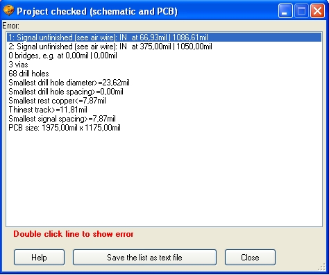
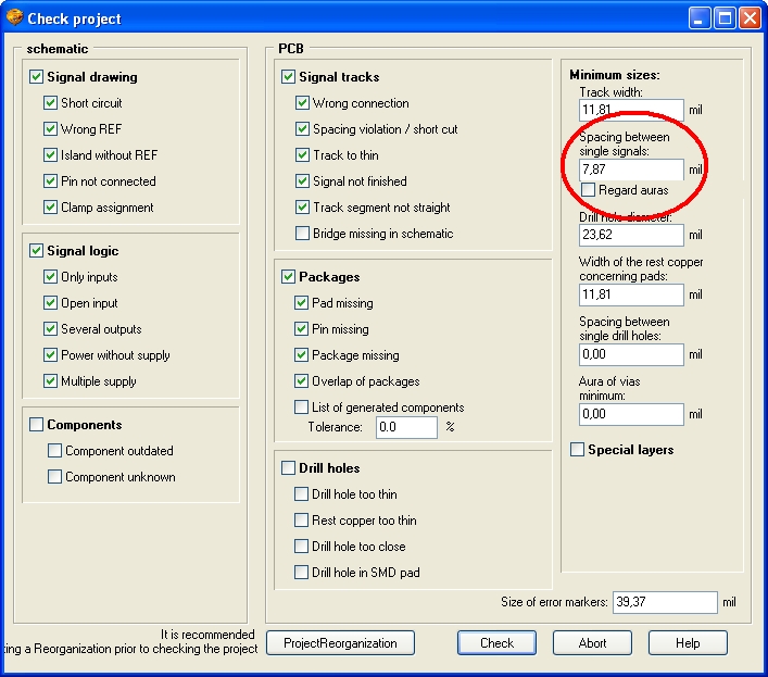
The dialog "check project"
Check components without a package, packages without components, short circuits, open circuits etc... Sometimes these situations are wanted or necessary. For example, if you only want to draw a PCB without having to think about drawing a schematic first.
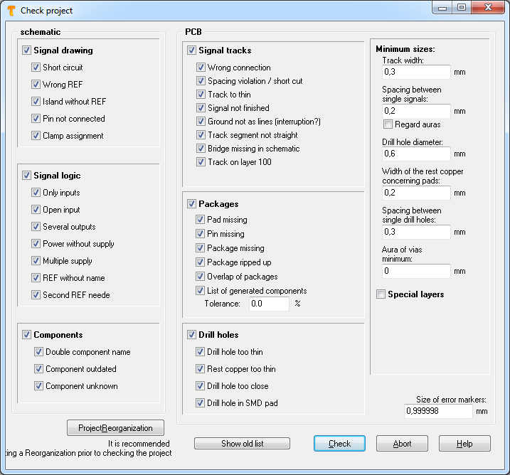
Nevertheless, to have everything proceeding the right way, you can use this function.
The result of the check
After pressing the "Check" button, all Design-Rule-Check-errors and Electrical-Rule-Check-errors will be displayed in an error list.
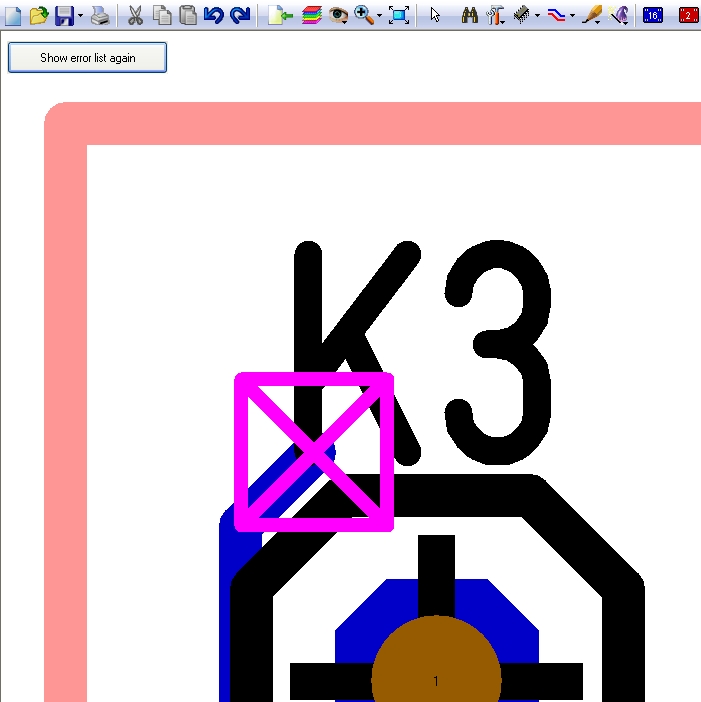
You can also save this list as a text file called TARGET.ERR into the current working directory. Doubleclick upon a certain line in the error list to fade out the list and get the error highlighted in the canvas by error markers.
Clicking M11 on an error marker a window will pop up giving a, short discription of the design error. Display the initial list again by clicking the button top left of the canvas "Show error list again".
After all errors are corrected, TARGET 3001! shows (for example) the following list:
0 Bridges
5 Vias
211 Drill holes
Minimum drill hole diameter: 0,6 mm
Minimum distance between drill holes: 0,3 mm
Minimum annular ring of solder pads: 0,235 mm
Thinnest track width: 0,3 mm
Minimum signal distance: 0,25 mm
PCB size: 160 x 100 mm
How to fade out or delete the error markers
The error markers can be faded out by deactivating layer #28. The Project-Reorganisation command deletes the check result and all error markers. Now a new "Check project" is required.
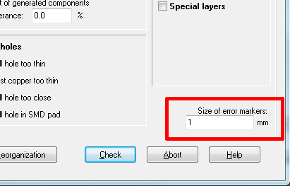
How to manipulate the size of the error markers
Please have a look bottom right of the main check project dialog:
Ignore spacing
As of V32, the check for spacing to other signals can be disabled for individual elements. This is interesting e.g. with an existing bridge in solder jumpers. If there is a standard connection in the jumper, which can be optionally scratched away later, then the check at this point always threw an error message because of a spacing violation:
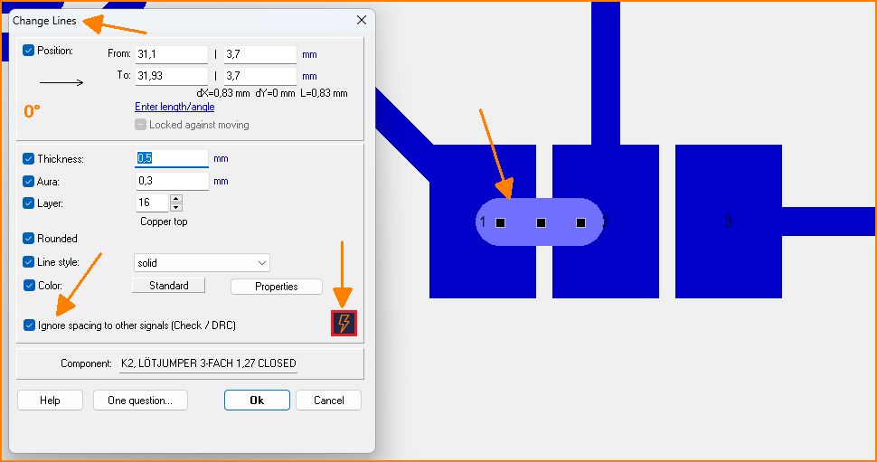
Ignore spacing
A lightning bolt symbol appears in the right margin to additionally illustrate the danger of this checkbox.
The meaning of the error messages
The following error messages might occur during the execution of the Electrical-Rule-Check:
Drillhole missing
A pad for example is placed on layer 100 which means that a drill running through all layers is expected but the drill diameter is zero. Or a it is placed on a higher layer in the sense of a padstack (layer number 101 and more) but the drill diameter is zero. Create a drillhole by defining it's diameter. Double click the pad M11 and enter a drillhole diameter in the flashing dialog. A SMD Pad being placed upon a layer beyond 100, e.g. layer 2, Copper bottom, sure does not require a drilling.
Aura too small
If in the "Check project" dialog to the right: "Aura of vias minimum" a value bigger than zero is entered, then the aura of vias in the layout at least need to have this width. If it is smaller, then this alert will appear. Doubleclick this via M11 and enter a value bigger than the one in the "Check project" dialog.
Drillhole too small
If in the "Check project" dialog to the right: "Drill hole diameter" a value bigger than zero is entered, then the drill hole of pads and/or vias in the layout at least need to have this width. If it is smaller, then this alert will appear. Doubleclick this via M11 and enter a value bigger than the one in the "Check project" dialog. It is to prove in the project that no drilling in the layout will be smaller than e.g. the smallest drill your pcb house is able to do.
SMD pad with drillhole
If a pad is placed upon a single layer lower than 100, for example only on layer 16=copper top or only on layer 2=copper bottom, it indicates a SMT constellation. So this is not a pad for a wired component where the pad would be on layer 100=through all layers. It is not a padstack too, which are defined on layers higher than 100. So if there is a drill within such a SMT pad this message appears.
Caution: If this hole is drilled through completely and copper is present on another layer, a shortcut can be the result! Delete the drill hole by hovering the cursor upon it and click M11. Change the drill hole diameter to zero. If you have placed the drill intentionally, please ignore the message.
Symbol outdated
The symbol of a component has a younger date in the libs/database than in the schematic. This doesn't necessarily mean that the symbol is erroneous (for Versions up to 15.5.0.17). Basis: Each symbol receives a mark telling about the date when the part had been modified latest. This mark we call the "LAST MODIFIED" entry. For the future we plan to subsume to this check only those symbols which had been befallen by a repair thus in fact had been erroneous and the error had been repaired at last modified date. Using menu option "Component/Replace components" you will be able to update the components within the project. For the symbols the property "LAST_MODIFIED" is compared, for the package the property: "LAST_MODIFIED_PACKAGE".
Symbol missing in database
For the check, whether a symbol probably is outdated it is crucial to find it in the database at all. The "Not Finding" of a symbol can be unobstructive.
Package outdated
The package of a component has a younger date in the libs/database than in the layout. This doesn't necessarily mean that the package is erroneous (for Versions up to 15.5.0.17). Basis: Each package receives a mark telling about the date when the part had been modified latest. This mark we call the "LAST MODIFIED" entry. For the future we plan to subsume to this check only those packages which had been befallen by a repair thus in fact had been erroneous and the error had been repaired at last modified date. Using menu option "Component/Replace components" you will be able to update the components within the project. For the packages the property "LAST_MODIFIED" will be compared, for the package the property: "LAST_MODIFIED_PACKAGE".
Package missing in database
For the check, whether a package probably is outdated it is crucial to find it in the database at all. The "Not Finding" of a package can be unobstructive.
Track on layer 100
Layer 100 and above are not meant for signal tracks though you can place them there. Signal tracks on layer 100 appear on all copper layers. Also within padstacks (Layers above 100) tracks can be placed. In most cases this is not senseful and the placement will be wrong. Tracks in general are placed upon copper layers lower than 100. This message is just a note because it might be possible, that you have placed the tracks there willingly. In this case please ignore this error message. Otherwise delete the signal tracks in question.
Wrong REF
A short circuit in the schematic. A reference symbol (REF) representing a certain signal name had been connected to a symbol representing a different name. Or a REF had received a signal name different to the one it represents in fact. Double click M11 allows adjustment in the flashing dialog.
If a (REF) is used without text display of its signal name, the signal name needs to be GND. Only the genuine ground symbol does not need a text. Just the signal name exactly needs to be GND. All other signals need the display of their name in the REF.
Sure you manually can assign any signal name other than GND. But this will lead to logical errors.
Example:
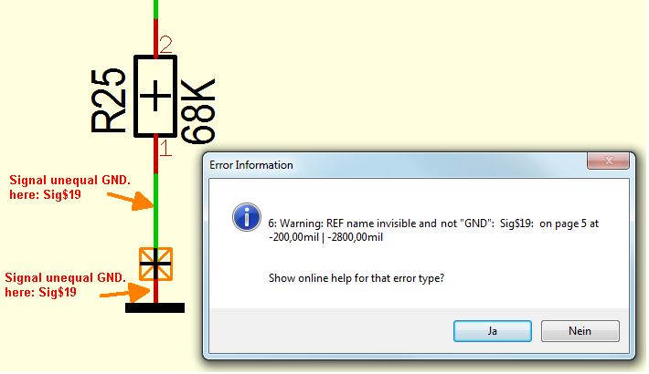
The signal name of the ground symbol and signal are different from "GND". But TARGET 3001! expects GND in this case.
Solution: Delete the signal segment, double click REF symbol (GND), change signal name to GND, connect new. Do a project reorganization (menu Actions) in order to make the error marker vanish, and do a project test again (menu Actions).
Track too thin
The prescribed track width is not reached. This value is requested as minimum width in the signal (schematic) or directly in the check dialog on the upper right. A copper layer can also require its own minimum width. The error message can occur with individual track segments or with signal polygons whose filling width is too small.
Bridge missing in schematic
In the layout a bridge had been created using keyboard key [b] for bridge or by the "tools" icon in the toolbar. This also could be a zero ohm resistor lacking a symbol in the schematic.
Illegal Padstack
A padstack had been created and used in the layout but deleted later. Or the pad which had used this padstack points at padstack 103, but this one is no more existant. All pads using this no more existant padstack need to be diverted to another padstack or to layer 100 (like a via).
Missing package
The schematic drawing contains a component which requires a package. The package however is missing on the PCB. Please place the missing package on the PCB.
Unfinished signal
The schematic requires connections which are incomplete on the PCB. Either individual solder pads of the signal are not connected or the signal is made of two or more signal islands. For checking, activate the pointer-option Mark signal islands ![]() When you click now M1 on a track, you can see exactly where the signal flow stops.
When you click now M1 on a track, you can see exactly where the signal flow stops.
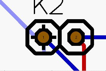
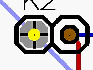
The first image shows a track which isn't connected correctly in the middle of pad 1. Optically this track is touching the copper thus seeming to be connected. In fact two separate signal islands are created which aren't logically connected to each other. Please see the correct connection in the following image:
Tracks are "sensitive" only at their endings. Whether TARGET 3001! recognizes two tracks as "connected" depends on the setting of the grid. See the following image of the X-ray view of a track:
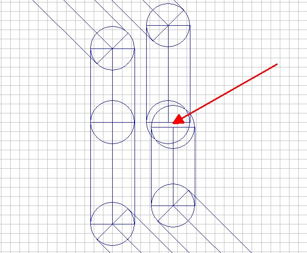
TARGET 3001! recognizes the track to the right side as "not connected" (see arrow), though their segments touch. The centers of their endings mustn't be placed more than half a grid apart from each other. Having lots of alerts in this respect we recommend to set the grid not too narrow.
Besides: Groundplanes in the layout do not carry on a certain signal. A groundplane is only supporting an existing track. See Groundplane.
.
Power without supply
This is an error message of the schematic.
No supplier of power is connected or defined as such! Please ask yourself:
1. Have I got a socket on my schematic? Only a socket can supply power to a circuit!
2. Do the pins of the supply socket which define +5V, VCC... show pin function "Power (supply)"?.
Note: Components without package proposal (PROPOSED_PACKAGE) are ignored in this respect (assumed as not existant).
In other words: To the power pin of a certain component (Power connection of a user) a signal might be connected but the pin it comes from (supplier) does not have this particular function "Power (supply)".
Example:
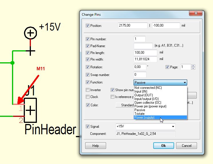
Several ICs are connected in a "+15V" net. Power comes by a PinHeader to the board. The Power Pins of the ICs have the function "Power pin (power input)" preset which is correct. But the pin functions of the connector are preset "Passive". In order to make TARGET understand that the power for the ICs is supplied by a certain connector pin, this pin needs to have the pin function Power (supply)
Click M2 on empty space first, a context menu flashes. Untick the first option "Always select entire component". Now click M11 on pin 1 of the PinHeader J1 from where the power is supplied. The Change Pins dialog opens. Change the function towards Power (supply)
This shows that even a simple dipole (connector, resistor, fuse...) does not carry this information . E. G. the function of a resistor's "Out"-pin needs to be set to "Supply".
Another example:
Say you have a NE555D Timer component whose power pin VCC correctly shows pin function Power pin (power input). A resistor shall be connected between this Power pin and its source, a Pin Header. Pin 1 of the resistor needs to be set to Power (Supply) because it is the source for the VCC pin of the Ne555. If this setting at the resistor pin is not made, you will get the error message "Power without supply". It is because TARGET wonders "What's the source of the power pin VCC of the NE555? Who provides power to it?" VCC is consumer, Pin 1 of the resistor needs to be defined as a supplier.
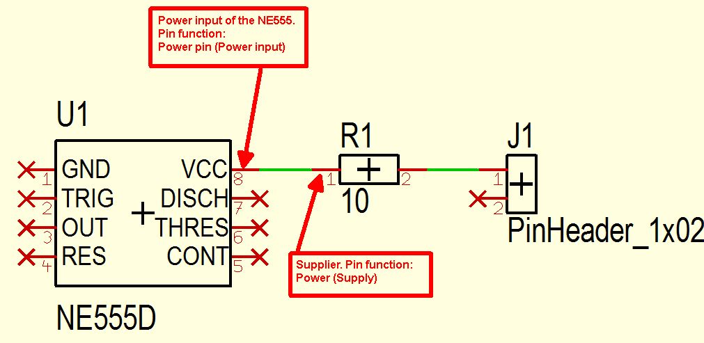
If the resistor was not there, you would need to set pin 1 of the PinHeader J1 Power (Supply) accordingly.
Important: Power signals normally are not treated with buses.
Special Case: Use of a virtual voltage source in the schematic only for simulation reasons
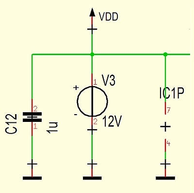
Bild: Use of a virtual voltage source in the schematic only for simulation reasons
In this setup a 12V voltage source was used. But this one is only meant for simulation. For the circuit it has the same meaning like a voltage from a power supply unit used in laboratories. This means there is no equivalent in the PCB layout. In reality on your PCB there would be some kind of a connector or similar of which the function of the poles would need to be defined as "Supply".
Note:
If VDD and VCC would be used with a common GND, TARGET unfortunately would not recognize, that the common GND would not make any trouble. You get a warning instead saying "multiple supply". One can ignore this alert.
Output error
An error message referring to the schematic. One signal either is fixed to several output or supply pin. A signal can only have one output or one supply.
.
Island without Ref Pin
Error message of the schematic. The signal in the schematic consists of several signal islands which optically seem to be connected. The connection in fact must be effected by reference symbols or by buses. If the error message appears nevertheless, please set the highlighting mode by the use of ![]() to "mark the signal island hit" and highlight by M1 all islands of a signal after each other. Danger: this error message might point at a short circuit in the schematic. Example: at a resistor both pins are connected to the same signal. TARGET 3001! recognizes two islands of the same signal and the autorouter would short circuit the resistor with other signal tracks. For localizing this error please highlight the complete signal by the use of the binoculars ("Find and select a Component or Signal"). Check the schematic in any case when this error message appears after using the "Check project" function. If you really don't find a different signal island, then please search for "orphan" signal track pieces, which might lay under an already existing signal track. Use keyboard key [s] (for select) several times when the cursor is close to a suspicious spot. Different elements being close to the cursor will flash though eventually invisible because covered by another element. If it flashes, press Enter and then delete it.
to "mark the signal island hit" and highlight by M1 all islands of a signal after each other. Danger: this error message might point at a short circuit in the schematic. Example: at a resistor both pins are connected to the same signal. TARGET 3001! recognizes two islands of the same signal and the autorouter would short circuit the resistor with other signal tracks. For localizing this error please highlight the complete signal by the use of the binoculars ("Find and select a Component or Signal"). Check the schematic in any case when this error message appears after using the "Check project" function. If you really don't find a different signal island, then please search for "orphan" signal track pieces, which might lay under an already existing signal track. Use keyboard key [s] (for select) several times when the cursor is close to a suspicious spot. Different elements being close to the cursor will flash though eventually invisible because covered by another element. If it flashes, press Enter and then delete it.
Only inputs
There is no defined voltage level on a signal, because only inputs are connected (signal is flowing). There must be a connection to a pin having the function Output (OUT).
Note: Components without package proposal (PROPOSED_PACKAGE) are ignored in this respect (assumed as not existant).
Open input
An input is flowing. Input pins of unused symbols must be connected. In case that the pin should really be unconnected, set it's function to NC (not connected).
Second REF missing
Error message of the schematic. A reference symbol (REF) was used whose property "NEED_2ND_REF" is set True. Such a REF requires a further REF as counterpart. The following IBF-REFs will be set by TARGET 3001! automatically when imported to the schematic: !SIG_IN, !SIG_OUT and !SIG_IO.
These REFs indicate some kind of flow of energy or information. That's the reason why they need a counterpart.
Short circuit
In the schematic:
Misconnected! Two signal tracks with different signal names wrongly had been connected. Or a pin internally has a different signal name to the one it is connected to. A signal needs to have an identical signal name in all it's segments (including pins). For checking it you can doubleclick each single segment of a signal in order to look out for the signal name and adjust it if different. In menu "Settings/Options" you can make TARGET 3001! display the signal name to every signal segment.
In the layout:
Misconnected! A soldering pad in the layout is connected to a different signal than required from the schematic. A signal needs to have the same signal name throughout all its segments including pads. For checking this you can double clicj each segment and look out for it's name and eventually change it. In menu "Settings/Options" you can display all signal names to the track segments.
Also internal connections in packages can cause short circuits. If a package has internal connections and different signals are connected to the corresponding pins, this message can appear too.
Attention 1: Pure spacing violations which also may lead to tangency and short circuits are not recognized by this check!
Attention 2: The grid size value is regarded for this check! Two tracks with their ends nearer than a grid can be seen as connected, even if they do not touch. Inexplicable short-cut messages can be removed by changing the grid.
Pin without a solder pad
There is a solder pad missing on the PCB for an existing pin in the schematic. Maybe you have deleted a solder pad afterwards from an existing package or you have used the wrong package. Delete symbol and package and import a new component both parts being consistent.
Solderpad without a pin
In the layout there is a pad with a pad number but there is no equivalent in the schematic. Maybe you have deleted a pin from an existing schematic symbol afterwards or you had used a wrong package to the symbol. Delete symbol and package and import a new component both parts being consistent.
Multiple supply
A signal is connected to several different power supplies, e.g. 5V and 12V. Please note: it is meant for GND too. On one net (in one signal) only one pin with "POWER SUPPLY" ia allowed. That's the reason to leave one pin function with POWER, the others showing the "SUPPLY" function shall be set to "PASSIVE" .
Not connected
In the schematic a pin is not or not correctly connected. Delete the last signal segment and place it new starting from the signal end towards the pin.
Every signal requires at least two real component pins. Reference symbols (e. g. SigIn, SigOut or Ground symbols) don't count here. As long as they themselves aren't connected with the pin of a corresponding component, you will get error messages. Watch this example::
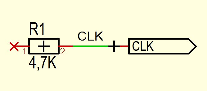
Image 1: Without a doubt the signal CLK is connected to the reference symbol SigOut, which has achieved the name CLK. Now start the "Project test" option in menu Actions.
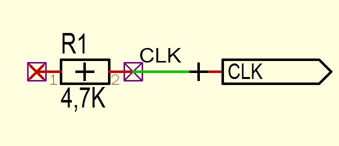
Image 2: Why does Pin 2 of the resistor get an error marker showing "Signal not connected?" Answer: The matching counterpin of the signal is missing. The bare connection to a reference symbol is not sufficient.
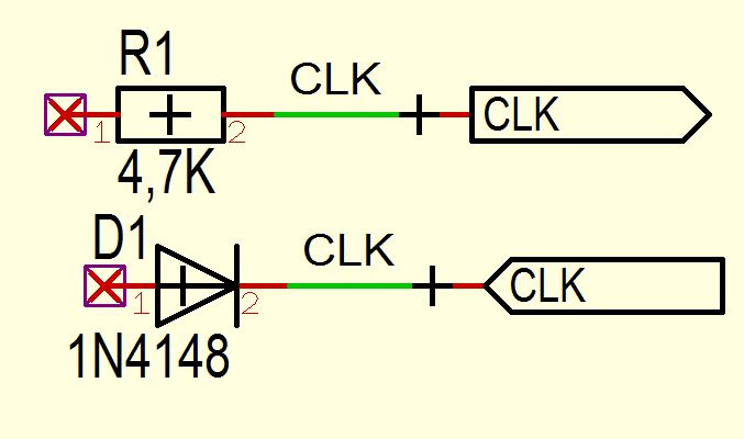
Image 3: Only the connection to a matching counterpin by the reference symbol SigIn makes pin 2 of the resistor connect properly. Is the signal connected further to the diode the whole signal is connected and the "Project test" function keeps quiet at this spot.
Maybe on the contrary it shall not be connected! In this case it might be good to avoid this error message (better: Warning message). Now set the function of the schematic pin to "Not connected (NC)" in the "Change Pins" dialog:

More signal islands than reference symbols
Every signal island must show its ownership visually to a signal through reference symbols or through a connection to a bus. In this case, at least one signal island is not connected to a reference symbol. Click on each of the signal islands with M1. Hereby, the tool "Mark signal island completely" must be activated. This error could also be named as double signal name! Also it might represent an unwanted short circuit. Please check all of your circuit for shortsafter this error message flashes. Two signal islands also occur if e.g. both ends of a resistor are connected to the same signal. The autorouter will connect both pads of the package like a short circuit. By the Design-Rule-Check the routed board additionally will be checked according to the settings of the "Design Rule Check" dialog.
Component outdated
There is a more recent version of a symbol or package in the libraries than the one used in this current project. Using menu option "Search and replace component shape" in menu Components allows an update of components within your project. For the symbols the property "LAST MODIFIED" is compared, for the package the property "LAST_MODIFIED_PACKAGE" is compared.
Age of symbol unknown
In the component properties the "LAST_MODIFIED" entry is missing or does not give a reasonable date. Replace the component by a database one.
Age of package unknown
In the component properties the "LAST_MODIFIED_PACKAGE" entry is missing or does not give a reasonable date. Replace the component by a database one.
Symbol/Package unknown
The symbol or the package can not be found within the libraries. For the check of the symbol TARGET uses the catchword under which the component was found when trying to import it and the property "COMPONENT_LIB". For the package the properties "USED_PACKAGE" and "USED_PACKAGE_LIB" are checked.
Spacing violation
A spacing violation occurs, if the copper of a different signal comes too close to the copper of the element in question or if it touches it. A spacing violation can be a short circuit in other words a short circuit in any case is a spacing violation. The minimum spacing of a copper element of a signal to all other copper elements of a "hostile" signal must be bigger than the biggest value out of the four:
- the minimum spacing in the "Check project" dialog
- the minimum spacing of the signal itself
- the aura of the element
- the layer related spacing (if a "special layer" for such is defined)
From Version V19.2.0.43 it is displayed from which value the minimum spacing is taken:
1. Spacing Violation: "CLK" <-> "RES" on layer 2 at 0mm | 0mm
2. Spacing Violation (Signal): "CLK" <-> "RES" on layer 2 at 0mm | 0mm
3. Spacing Violation (Aura): "CLK" <-> "RES" on layer 2 at 0mm | 0mm
4. Spacing Violation (Layer): "CLK" <-> "RES" on layer 2 at 0mm | 0mm
When checking the "Spacing between single signals" the "Regard auras" box needs to be ticked if the spacing shall apply including the aura.
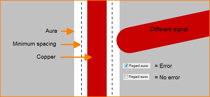
Image 1: The effect of "regarding the aura" in respect to a spacing violation.
Layers with different spacing rules (special layers) are to be found in the check project dialog at the bottom right.
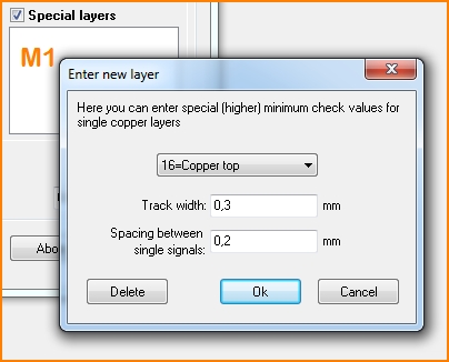
Image 2: Define a layer, to which different checking parameters shall apply (Special layer).
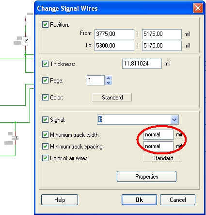
If your layout according to the rules of a PCB manufacturer gets checked against a general signal spacing of e.g. 0,15mm, the security needs of signal "240V" indeed might be higher. Close to signal "240V" a wider minimum spacing needs to be defined in the signal dialog. If a track "+5V" (mainly located in a low volt area of your layout) also touches an area of line voltage then the "+5V"-tracks in this area should get a bigger aura.
The following images show 2 "hostile" elements and their auras (aras can overlap in general):
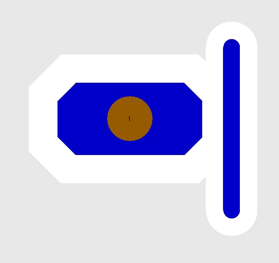
Image 3: A soldering pad to the left and a track segment to the right
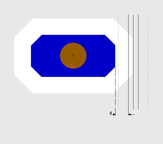
Image 4: Track segment touched by M1H for showing it's phantom lines...
If spacing d between the elements is smaller than the parameter in the "Check project" dialog, TARGET 3001! alerts a spacing violation. The track to the right might be OK with the distance to the pad. The pad on the other hand has a bigger aura which overlaps the track. From the Pad's point of view the spacing to the track is too small.
Note: Use these error messages to check whether your circuit has short circuits. If both pins of a resistor are connected to the same signal, a signal island is created. The autorouter therefore short-circuits the two solder pads of the according package symbol.
Ground plane not converted into lines
Error message in the layout. Sometimes it may happen that by incident you create areas within a groundplane which are isolated from the ground signal like an island. Elements connected here give the impression of being connected to ground but in fact electrically they aren't. A conversion of the ground plane to lines helps because it needs a definition of a line width which cares for the existance of copper "corridors", ligaments, at least having the strength of the line width. So it is made sure that the ground potential unobstructedly can travel around all areas of the ground plane. If those corridors do not exist or might be too narrow for production unconnected ground islands might occur. Remember: Gerber data will make a light finger move around to exposes all remaining copper to light. If there are corridors being too narrow the light finger makes a jump and by this means cuts off the area behing him. So please check by converting your ground plane into lines (menu: Action/Ground plane/Generate ground plane... Tab "Convert ground plane into lines") whether Ground islands exist. If yes, connect them properly or widen narrow copper "corridors". Also see: Groundplane#Tracks_leading_a_groundplane_signal_always_should_be_routed...
Here is an example: Image 1 gives the expression that all GND is connected to the plane. Image 2 shows a corridor being too narrow for production, see arrow so that a not connected island remains (green). The whole design might be corrupt. By a conversion into lines the island will be recognized and the design can be adjusted.
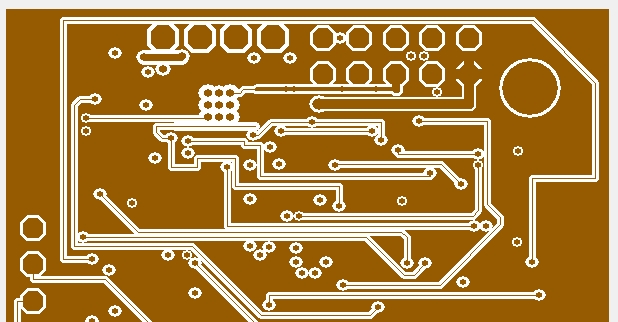
Image 1: The brown area GND seems to be connecting everywhere.
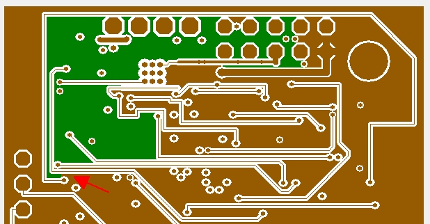
Image 2: One ligament is too narrow which causes misconnection when produced that way, see arrow.
Polygon too chunky
A ground plane in lines (as a grid) offers production advantages in galvanization and in respect to electromagnetic performance of the signal. In addition to the track width you can define the distance of the mesh, the grid spacing. NOTE: If the grid spacing gets too wide, the polygon will not be able to convey the signal any more.
The limit is:
Grid spacing > Minimum Drill hole diameter + 2 x Width of the rest copper concerning pads
If you use the "Check project" routine or if you "Compute Air Wires (Ratsnest)" such a widely spaced polygon grid can not put the signal through to it. So there will remain an air wire and the soldering pads in question need to be connected by a signal track manually.
The following message could appear when using the "Check project routine"
"Signal-Polygon too chunky: GND on layer 2..."
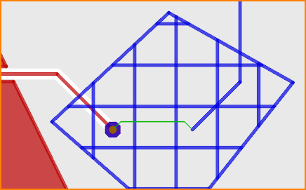
Copper top: The ground plane is gridded too wide. Please double click the polygon and enter a smaller grid value to the dialog.
Please also see Signal polygon
Warning: Ground plane check disabled, disrupted planes possible!
Before checking the project you had not ticked the box at Ground not as lines (interruption?) in the check project dialog (see image). That means you had switched off this particular checking routine.
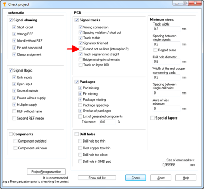
Image: Ground not as lines (click image to enlarge).
Therefore TARGET can not check whether there are ground plane areas which aren't linked to the whole plane. You would manage such a linking by converting your ground plane to lines. Please tick the box mentioned in order to activate this checking routine. This will make this warning vanish. Now you would get warned if your ground plane was not converted to lines thus would keep the danger of areals not being linked to the entire ground plane. See also the previous article.
Component outline defective
This message appears, if the outline of a package or a symbol drawing is not closed properly. Make use of the hash-key [#] for X-raying your drawing. All frictions get visible quickly:
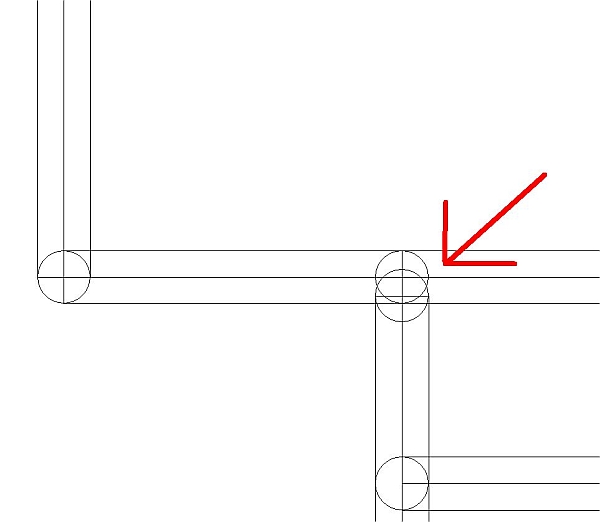
Image: Component outline defective
Package ripped up
This message only refers to the layout. For example a pad is displaced and does not match to the grid. In other words elements of this package have been displaced so that the part appears different from it's source in the database.
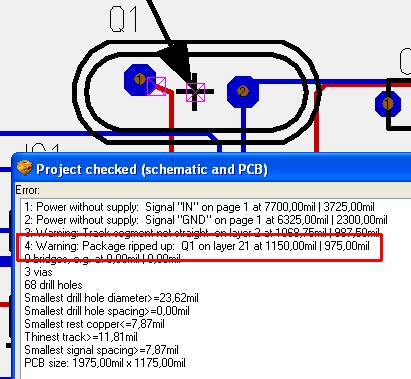
Image: Package ripped up (left pad moved further left)
Either you willingly have displaced the part and wish to leave it as it is or you redo the genuine state. Both will be OK. You will delete the error marker by deleting the entry "PACKAGE RIPPED UP" as well as it's value "TRUE" from the property list: hover the mouse to the handle cross of the package, press [s] as long as the handle flashes, press [e] for edition and click the properties button in the dialog. Now delete the whole line "PACKAGE_RIPPED_UP" left and right.
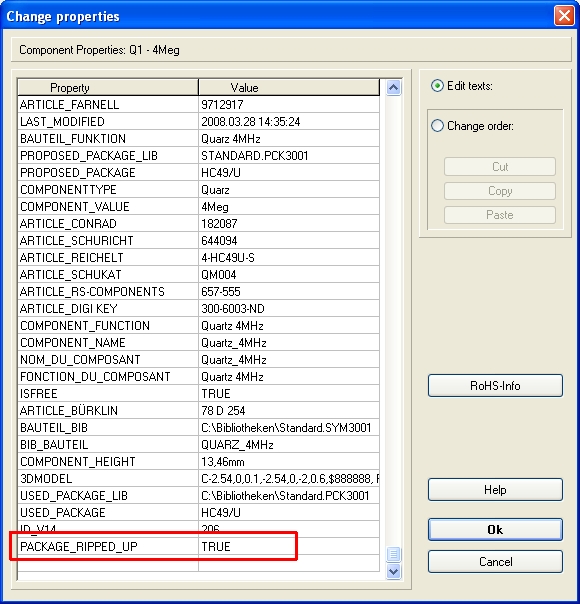
Image: Property list of the component being ripped up. Delete the line framed red. Now the error marker in the layout will vanish.
Package Overlap
Two package outlines are overlapping. This would cause conflicts when assembling. Displace the package marked to a better position. If a package shall be excluded from this check (e.g. if the PCB outline itself was imported as a "package", it would have conflicts with all other packages), then this component must get the property "IGNORE_OVERLAP" with the value "YES".
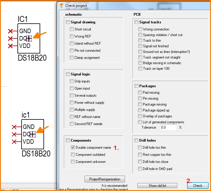
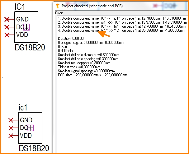
Double component name
While having changed a component it was possible to create a component name double. Maybe by mixing up capital- and lower case writing. From V18.2.0.64 there is a check routine: "Component name double".
Solution: Double click on the handle cross of a symbol and adapt its component name in the dialog accordingly.
Click a purple error marker to get the following error information dialog:
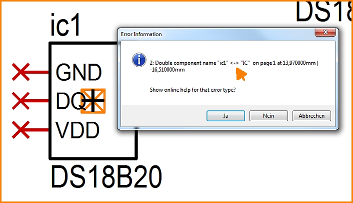
Image: Error marker => Error information
Width of the rest ring of a soldering pad
If the soldering pad diameter is 1 mm and the drillhole diameter is 0.6 mm, a rest ring of 0,2 mm results. As long as a rest ring remains at all, a plating through happens. A drillhole without rest ring thus doesn't get galvanised (=no plating through). You can widen the rest ring by either reducing the drillhole diameter or widening height and width of the pad. Double click on the pad opens the dialog for edition.
Spacing between drillholes
If the distance between two drillholes (center to center) e.g. is 1 mm and the drillhole diameters are 0.8 mm and 0.6 mm, a spacing of 0.3 mm results. If you have calibrated the "check project" dialog regarding this aspect to 0.3mm you will get an error message that the drill would be too close, if the distance is smaller. Either you widen the distance between the drills or you reduce the calibrating parameter in the check project dialog to make this error message vanish.
Wrong signal at clamp: CMP / Pin X "Sig$1"
Error message concerning cable harnesses. The component in question has property "IS_CLAMP" activated. To a certain clamp signals are connected, which are recognized an not belonging together e.g. "1.1", "1.2", ... "1.99" etc.. In case you do not intend to check clamps or cable harnesses, delete the components property "IS_CLAMP" or switch off the checking of the "Clamp assignment" in the Check project dialog.
File "C:\Programs\ibf\CounterParts.txt" missing
Error message concerning cable harnesses. Set in Settings (Registry) the entry "Cable functions in main menue" to "No" (position 8 from the bottom of the list)
Track awry
This is a warning only, no error. A segment of a trace is neither vertical nor horizontal nor in a 45° grid. Up to V19.8.0.94, only segments that were at least twice as long as their own line width were examined. From then on, all awry segments are reported, including short thick segments. Since V20.2.0.19 awry tracks are reported, if they are at least twice as long as their width. And tracks that are at least half as long as their width, if they deviate more than 3°. Shorter segments are not reported at all.
Design-Rule-Check error messages
Most of them are spacing violations or tracks that are too thin. TARGET 3001! regards the values entered in the DRC dialog as well as the properties of signals "MinimalWidth" and "MinimumSpacing".
Check - Aura - Track Spacing
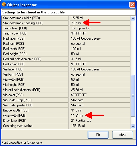
The Aura is the security spacing a signal has towards a groundplane you might consider to create. The Standard track spacing (PCB) is the spacing a signal in general at least shall have towards another signal. Aura and Standard track spacing can vary e. g. if you would like to have a slightly bigger aura around pads for making soldering easier than you need to have alongside the tracks. TARGET 3001! offers setting options in the "Object inspector" which you open by menu "Settings/Settings (Project)..." The following settings are predefined as default:
TARGET 3001! uses these settings as "normal" signal properties in the schematic.
These values are overtaken to the layout at first but they can be adapted at any time.
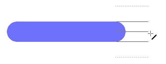
When placing tracks you'll see a phantom image having hatched lines aside. This hatched lines represent the higher one of both values, by default the "Aura". If you set the value "Standard track-spacing (PCB)" higher than the value "Aura width", then the hatched line represents the standard track spacing.
In menu "Action/Check project..." to the right you see the field "Standard track-spacing" preset by 7.87 mil. The aura shall not be regarded in this checking situation, the box remains unticked:
In the check result TARGET 3001! marks all spots, where two varying signal leading elements have spacing to each other smaller or equal 7.87 mil. Whether the aura of one of those touches a signal element (e.g. a track) is disregarded according to this setting.
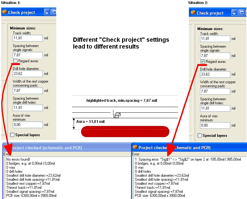
The following image might illustrate the situation. Starting from the center of the image you see two signal tracks, the upper one highlighted so that the manually set aura of 11.81 mil can be seen in hatched line. It touches the track beneath (red). Predefined is a minimum spacing of 7.87 mil against which the project now gets checked.
Situation 1 leaves the aura disregarded which does not lead to any error message, because the minimum spacing (7.87 mil) between the signal leading elements is kept. Shall the aura be regarded, the box in the check project dialog needs to be ticked see situation 2. Now TARGET 3001! alerts a spacing error because the aura of the upper track touches the copper of the lower track.
.


