Reverse Engineering: Difference between revisions
No edit summary |
No edit summary |
||
| Line 1: | Line 1: | ||
== | |||
== In edition "design station"... == | |||
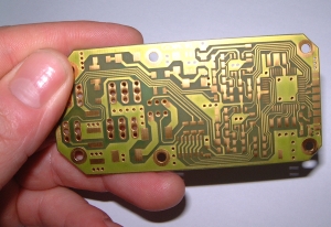
[[file:Reverse.jpg|left]] From version V15 the TARGET 3001! flagship, the '''design station''', offers a new professional "Reverse Engineering" solution.<br><br> | [[file:Reverse.jpg|left]] From version V15 the TARGET 3001! flagship, the '''design station''', offers a new professional "Reverse Engineering" solution.<br><br> | ||
| Line 10: | Line 10: | ||
The company Diagnosys offers the PCB diagnosis system "Pin Point", which creates the netlist needed by an electronic sampling process. Using a special heuristic method in TARGET 3001! the complexity of this ratsnest is reduced to a minimum. Components and signals get spread over different schematic pages by a '''Simulated Annealing''' algorithm. From there a new PCB layout can be created using all tools of TARGET's PCB creation. This feature only is available in edition '''"design station"'''. | The company Diagnosys offers the PCB diagnosis system "Pin Point", which creates the netlist needed by an electronic sampling process. Using a special heuristic method in TARGET 3001! the complexity of this ratsnest is reduced to a minimum. Components and signals get spread over different schematic pages by a '''Simulated Annealing''' algorithm. From there a new PCB layout can be created using all tools of TARGET's PCB creation. This feature only is available in edition '''"design station"'''. | ||
== Reverse engineering in | |||
== Reverse engineering in all editions == | |||
Revision as of 09:04, 12 July 2018
In edition "design station"...

From version V15 the TARGET 3001! flagship, the design station, offers a new professional "Reverse Engineering" solution.
The problem: A customer has an old, defective PCB bare of any documentation or CAD data. Unfortunately this circuit controls his Bucket Wheel Excavator, Rail Car, Ferry Boat, Aeroplane, Locomotive, Rack Railway or whatever industrial equipment standing non-productively idle because of electronic damage. The manufacturer is no longer on the market, service companies are not to be found. So if you don't want to scrap your machinery the only way is rebuilding the defective PCB. But even for experienced developers this method is combined with enormous difficulties though there might be only few parts in the game.
The solution: By the help of a netlist TARGET 3001! creates a schematic including the part namings as well as the signal names. A new PCB layout now can be "cloned" from the old.
The company Diagnosys offers the PCB diagnosis system "Pin Point", which creates the netlist needed by an electronic sampling process. Using a special heuristic method in TARGET 3001! the complexity of this ratsnest is reduced to a minimum. Components and signals get spread over different schematic pages by a Simulated Annealing algorithm. From there a new PCB layout can be created using all tools of TARGET's PCB creation. This feature only is available in edition "design station".
Reverse engineering in all editions
Now if you want to re-edit or modify the layout your job is to redraw the complete layout (Reverse Engineering). In this respect it is fine to use an image of the layout as a default in TARGET 3001!. "But an image of the layout is only a kind of painting which will not provide any pad and track or groundplane information" you might argue. You are right. But nevertheless an image as a default is a great help for locating packages and redrawing the connections. Place the image beneath your layout in TARGET 3001! (upon layer 0=area bottom) and place all elements upon it. Later when your layout is finished, you can delete the image.
Take a bitmap (= an image having the file extension *.bmp) to your clipboard and insert it into a color filled rectangle which you had placed upon layer 0 .
Use the "transparent...opaque" slider in the "Load picture into rectangle" dialog to determine the opacity of an imported image. So you can look a little through your photo of "copper top" to see what is happening on "copper bottom". Exact placement of housings and traces on both sides is then easier.
Now place all landmarks (pads), tracks and all other elements upon higher layers. First make sure that your visible screen is set to real size in mm or inch. See menu "Settings/Settings / Options". In this dialog look for "Usable monitor size" and enter the measurements of your screen (take a fold-rule and hold it on screen to figure it out). Otherwise you might suffer deformation. Now act as follows:
How to proceed
1. Step:
Measure the dimensions of the default as it shall come out in reality. Create a bitmap of the layout you have. A scan of a board might have advantages against a handmade photography because of not showing distortions which (slightly) might appear when taking a photograph. Sure you also might use a plot of the layout. Our example board below has a real height of 43,00 mm and a width of 90,00 mm. The cut tips we ignore at first:
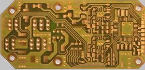
Image: A 100% scale scan of your layout
2. Step:
Open TARGET 3001! and select "Create a new PCB without schematic". Now draw a PCB outline on layer 23=Outline using the above measurements. If you want you can use the "outline assistant" in Menu Actions / "PCB Outline Wizard".
You can toggle from imperial scale to metric and back by the use of the function key [F4].
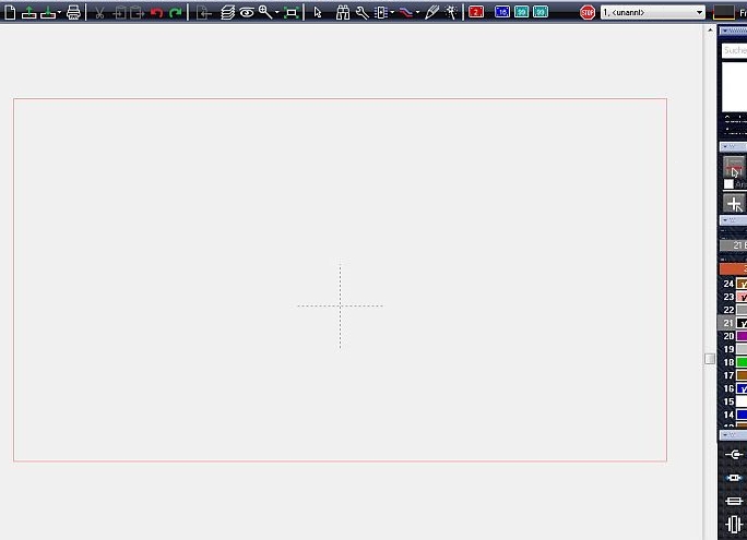
3. Step
Now draw a filled rectangle...
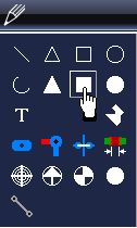
...upon layer 0=Area bottom having identical measurements. Don't use "open rectangle" because later the import of your bitmap from the clipboard does not work:
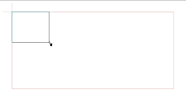
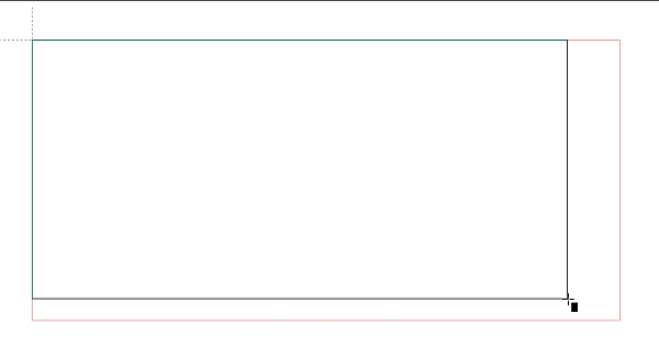

You might adjust the measurements of the filled rectangle by doubleclick on it and entering to the dialog:
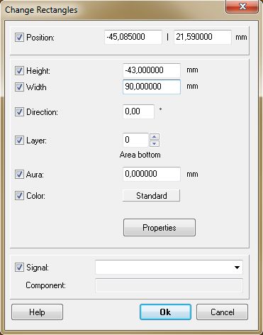
After you have made your entries (you also might have dragged your rectangle to fitting size) you'll see the filled rectangle coloured red. Now please highlight it (mark it) and see it in light red.
4. Step:
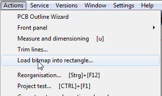
Take the bitmap of your aimed layout to your clipboard like you always do in Windows and open the TARGET 3001! Menu Actions / "Load bitmap into rectangle".
As a result your PCB photograph is projected onto the highlighted rectangle. You will figure out that the bitmap only needs to have the same height/width relation. the overall size does not really matter. The bigger the bitmap is, the higher the resolution will be. Our example shows the positioning (populating) side of the board. The image should be shifted to layer "0, Area bottom" (double click on the image and enter "Layer 0" to the opening "Change rectangles" dialog).
5. Step:
Now you immediately can start importing components from the database and to place them on the layout at correct position. On the right side you see there had been used a TQFP44 device - get one from there...
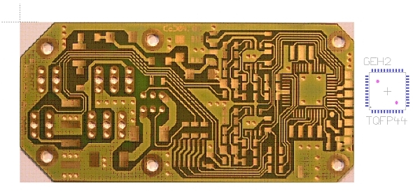
...and place it. Zoom in deeply and place the package exactly. Be supported by the x-ray function. Toggle the hash-key [#] on the keyboard.
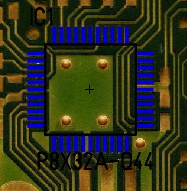
6. Step:
Place a smd resistor with a package 0805 and rout the tracks between the pads.
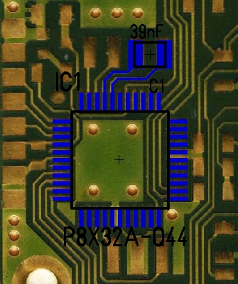
Further steps:
Get in each component package bit by bit and connect them. In our example you see the results in blue, because it's the standard color of layer 16=copper top. If you want to use the bottom side of the layout, you must get in the bitmap already in mirrored shape. The effect is, like usually in TARGET 3001! that you see from top through all layers to the bottom of the board. At the end cut the tips of the outline on layer 23 by using the drawing tool to get the same outline like the default PCB.
Now the placement of packages and connecting tracks is your job...
You can use this function in the schematic also. It is located in the same menu and works the same. It is meant for inserting logos etc. to the schematic. For the fact that the schematic view does not offer drawing on different layers there is unfortunately no chance to overlap signals to the image.
