Panel: Difference between revisions
No edit summary |
|||
| Line 21: | Line 21: | ||
Use function "[[Undo]]" to reduce the panel bit by bit beginning from below right. This function works within the [[Editions and prices|Pin-Limitation]] of any TARGET 3001! edition. So in a "Light" Edition (400 Pins/Pads) you can not set a project of 250 pins as a panel because the second piece would already exceed the pin limitation. | Use function "[[Undo]]" to reduce the panel bit by bit beginning from below right. This function works within the [[Editions and prices|Pin-Limitation]] of any TARGET 3001! edition. So in a "Light" Edition (400 Pins/Pads) you can not set a project of 250 pins as a panel because the second piece would already exceed the pin limitation. | ||
[[Image:nutzen5.jpg|none]] | |||
Between the boards, mills on layer 25 (milling) are drawn here manually. For a 2 mm wide cutter, 2 mm wide brown lines were used. Small ligaments were left as predetermined breaking points. Please discuss with your PCB manufacturer how the PCBs are to be separated afterwards and how this should look in your data. | |||
== Merge several layouts to one PCB == | == Merge several layouts to one PCB == | ||
Revision as of 16:21, 12 March 2018
General
A panel is a multiple placement of projects into one compound. It can be the same project multiplied or different ones having different shapes. The aim is having a maximum utilization of the process format when producing PCB. In TARGET 3001! you easily can multiply your project and not having the numberings counted up (as it is usual in TARGET 3001! when copied and pasted).
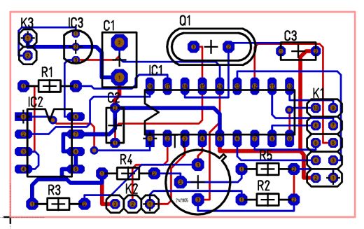
Example pic.T3001
We start from our example project pic.t3001. After routing it, it shows as follows:
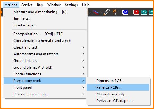
The function "Set a panel" please find in Menu Actions / Preparatory work / Set PCB as panel...:
After a click on this entry the following dialog opens.
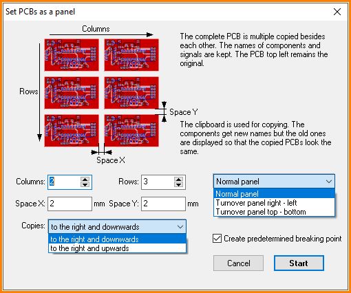
After entering your individual settings (we left the standard settings), the following picture shows:
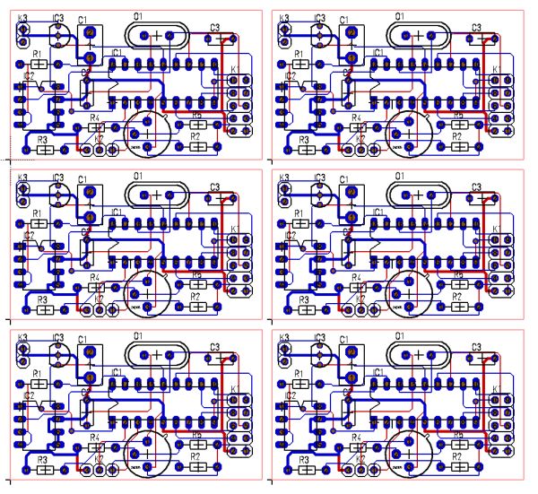
Use function "Undo" to reduce the panel bit by bit beginning from below right. This function works within the Pin-Limitation of any TARGET 3001! edition. So in a "Light" Edition (400 Pins/Pads) you can not set a project of 250 pins as a panel because the second piece would already exceed the pin limitation.
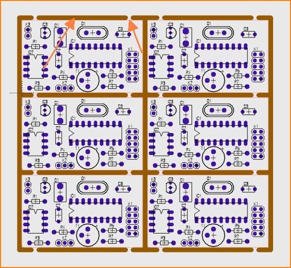
Between the boards, mills on layer 25 (milling) are drawn here manually. For a 2 mm wide cutter, 2 mm wide brown lines were used. Small ligaments were left as predetermined breaking points. Please discuss with your PCB manufacturer how the PCBs are to be separated afterwards and how this should look in your data.
Merge several layouts to one PCB
Maybe you want to merge two (or more) layouts to one PCB, for producing two or more small PCBs at a time. Principally it works by the use of the clipboard from one project to another. However the components of the layout added are renumbered automatically because TARGET 3001! does not accept two identical component names within one project. R1 of the first layout will be renamed to R12 on the second layout and so on. This might be unwanted in respect to the second layout.
There is a way to keep the numbers so that R1 can appear twice or more:
Open your project which you like to copy and select menu "Actions/Set PCBs as a panel". Internally the component names get adjusted like explained above but the texts shown get separated and become functionally changed from "Component name" to "Normal text". The earlier names within the text field are kept. Now copy such a "panel" layout, created by the menu mentioned, to your other layout. So you have two different layouts within one PCB-Project and keep identical component namings.
When pasting the layout by the clipboard you give new names automatically to all signals if you get asked for it. So there don't appear unwanted air wires between the PCBs.
Merge several layout modules to one PCB
Say you have created several small layout projects which you now wish to merge to one main project by copy and paste. Act like described above: Create at least a double panel. Here a copy from the initial project is made having the property of holding the component names. Now take such a copy (the original always is the top left one) to your clipboard and paste it to your desired layout.
Catch words:
Panelize different pcbs, multi-pcb, pcbs all in one, more drawing into one board, combining pcbs, pcb group, module layout, copy and paste, panelization.
