Pin: Difference between revisions
No edit summary |
|||
| Line 16: | Line 16: | ||
== Pin Options == | == Pin Options == | ||
The pin options dialog opens when pressing key [o] after selecting the '''"Place pin"''' mode from schematic menu "Elements". It is meant for defining a pin's properties for now and future placements.<br> | The pin options dialog opens when pressing key [o] after selecting the '''"Place pin"''' mode from schematic menu "Elements". It is meant for defining a pin's properties for now and future placements. These placements are meant only for the creation of a new schematic symbol. All other pins you will import to the schematic as part of existing symbols through the component database. Even if a component has only one pin and one pad (C1x1)<br> | ||
[[Image:e_PinOptDlg.jpg|none]] | [[Image:e_PinOptDlg.jpg|none]] | ||
Revision as of 13:53, 18 January 2013
A pin in TARGET 3001! is the electric connection terminal of a schematic symbol:
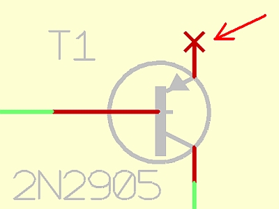
Place a pin when creating a schematic symbol
You can reach this mode...
by [1] or
by "Place Pin" in menu "Elements" or
by the icon ![]() .
.
Leave this mode...
by [ESC] or M12
What you can do...
You can place free pins with M1 clicks or by pressing [1] in pointer mode. Free pins are only used when defining new symbols which shall be saved as a component into a library. The pin numbers are incremented automatically. Press [o] (for pin options). Place the ultimate pin by [Return] or [Esc]. It is possible to change the pin number, the form and the function of the pins by pressing M11 in connection mode or with [o] for options. The following Options dialog shows some info about the component - and signal assignment. Other entries have the following meaning (release button ![]() in the pointer toolbar before doubleclicking a pin):
in the pointer toolbar before doubleclicking a pin):
Pin Options
The pin options dialog opens when pressing key [o] after selecting the "Place pin" mode from schematic menu "Elements". It is meant for defining a pin's properties for now and future placements. These placements are meant only for the creation of a new schematic symbol. All other pins you will import to the schematic as part of existing symbols through the component database. Even if a component has only one pin and one pad (C1x1)
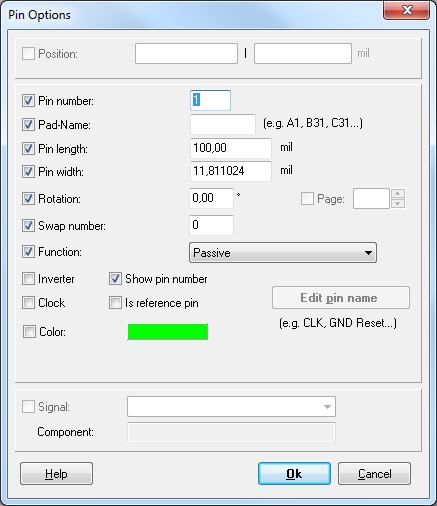
Pin number: The connection between the pin in the schematic and a pad in the package is this number. One of the most important informations a pin carries is the Pin number. Pin names are not regarded.
Pad names like A1-A20 and B1-B20 and C1-C20 are not regarded.
Inverter: The pin gets an inverter point.
Function: Defines the function of the pin. Select from the following:
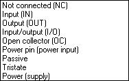
Not connected (NC): Pin is not connected (not used)
Input (IN): Pure Input
Output (OUT): Pure Output
Input/output (I/O): Changing input and output
Open Collector (OC): open collector output (open drain)
Power pin (Power input): Power supply of a component
Passiv: Pin of a passive element or function not clearly defined
3 States(Tristate): Output, which can achieve high-Ohm-impedance
Power (supply): Power supply of a PCB e.g. a connector supplying power to the PCB. Or the output of a voltage controller (e.g. 7805) which supplies others
Power pin means that this is a pin that needs power.
Power (supply) means that this pin gives power. Normally a connector pin is set to Power (supply). Power comes through this pin onto the PCB. Also pin 2 of a 7805 is a power supply pin. It supplies the other ICs with power. Their Power pins are consumer pins.
Clock: A little arrow shows that this pin is a clock input.
Swap number: Pins within the same symbol or gate and with the same Swap number greater than zero can be swapped with this pin.
Show pin number: Shall the pin number be visible? Useless for resistors, useful for ICs.
Is reference pin: If this box is checked, the pin is not representing a pad in PCB but is a signal reference pin such as used for ground symbols. This box shall only be used, when creating reference symbols for the reference symbol library.
Edit pin name: The dialog for the pin name will be opened.
Change Pins
The change pins dialog opens after M11 ohn a pin with the intension to change it. The dialog looks similar to the "Options" dialog but the entries refer only to this singular editing action.
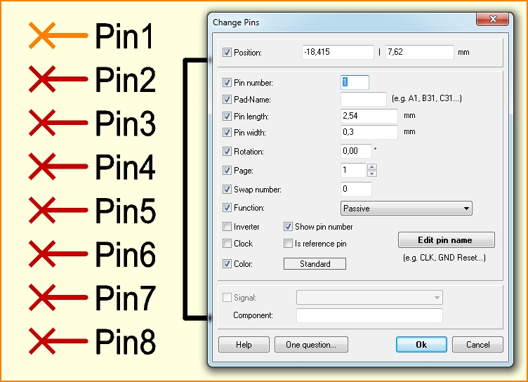
Position: Shows absolute coordinates.
Pin number: Shows the pin number.
Pad name: If the naming of the pins within the package is alphanumerical, (e. g. A1 - A32, B1 - B32, etc.), here you can drop those names. The pad name must be identical to the one of the corresponding pad of the package. The pin number must be identical (e. g. pin name of package A1= pin number 1, A32=32, B1=33, B32=65, etc.).
Pin length: Shows the length of the pin from starting at the cross.
Pin width: Shows the width of the pin.
Rotation: Shows the orientation of the pin. The cross is the reference point.
Page: Shows the actual schematic page.
Swap number: Pins inside the same symbol with the same swap number can be exchanged with this pin (for example: two inputs of an OR-Gate, the exchange number must be higher than 0).
Function: The following pin functions can be selected:
- Not connected (N/C): pin not used (not connected)
- Input (In): Simple input Output (Out): Simple output
- Input/Output (I/O): Pin changes its state
- Open Collector (OC): open collector (could also be open drain)
- Power pin (Power input): Power supply input of a component
- Passive: Pin of a passive element, the pin function may not be clear.
- Tristate: Output, that exhibits three states: High, Low, and Open (disconnected). This open state is called high impedance (or high Z-state).
- Power (Supply): Power supply input of the circuit or power supply output of a component (for example: 7805).
Inverter: Enable this feature if the pin is an inverter. The symbol shows the inverter sig at its end.
Show pin number: The number of the pin (= Component-Pin-Nr.) is shown in a small size on the side of the pin.
Clock: A small arrow is inserted at the end of this pin, if it has some clock function (clock input/output).
Is reference pin: This feature means that the pin is not representing a solder point, but is used an a signal name reference (for example: for connections used over several schematic pages (reference symbol)). Can be set first to [Y] during export!
Color: Define color of a pin independently of predefined color. Is color white (R=255, G=255, B=255) chosen, the predefined standard-color is used. If you wish color white although, you need minimal offset from the above mentioned RGB characters (just one point fits).
A name is generated while creating a pin. This name can be selected separately to be renamed or moved. If you need for the logic of the circuit only the name of the pin but not the pin number please change the name and delete it with M1 and [Delete]. It will remain invisible.
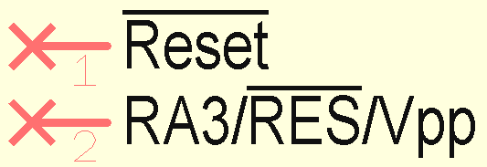
The pin name can also have an overbar. The pin name starts with a vertical bar then |. For example |Reset. The complete pin name has an overbar then. The overbar can also start within the pin name or end there: RA3/|RES|/Vpp. In the middle of the pin name has the word RES an overbar. Only one overbar can be used within a pin name.
Pin Swap
You can reach this mode...
by "Pin Swap" or in menu "Actions" or
by the tools ![]() .
.
Leave this mode...
by [ESC] or M12
What you can do...
Click the two pins or pads of the same symbol subsequently with M1. Both pins have to have the same non-zero swap number. In the schematic only the two pin numbers are exchanged. In the PCB the connected tracks are dragged along like rubber tracks. Caution: Short cuts are possible.
