Pin: Difference between revisions
| Line 72: | Line 72: | ||
== Pin Name == | == Pin Name == | ||
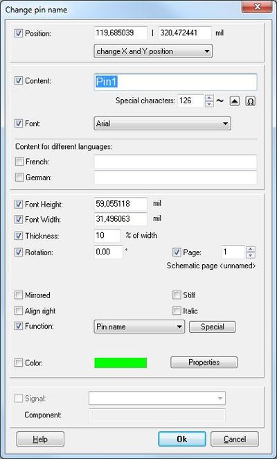
The Pin Name is the [[Text]] concerning a connection pin in the schematic showing its function e.g. GND or CLK or RES. Contrarily to the pin number it is a real individual data element in TARGET 3001!. It is placed or edited by a double click [[M11]] on the Pin in question. The opening dialog is named: "Change Pins". | The Pin Name is the [[Text]] concerning a connection pin in the schematic showing its function e.g. GND or CLK or RES. Contrarily to the pin number it is a real individual data element in TARGET 3001!. It is placed or edited by a double click [[M11]] on the Pin in question. The opening dialog is named: "Change Pins", see above. In this dialog please find button "Edit pin name" used to open the following dialog:<br><br> | ||
In this dialog please find button "Edit pin name" | |||
| Line 93: | Line 87: | ||
Don't mix up Pin name and [[Pad name]] which is a alphanumerical naming of pads arranged like a matrix e.g. in BGAs or connectors (A1, A2, ... B1, B2, ... B31). Thus a Pin additionally to its Pin name can have an alphanumerical Pad name which will be displayed in schematic and layout instead of the Pin/Pad number. The Pin number nevertheless internally is kept as the internal link between pin and pad.<br> | Don't mix up Pin name and [[Pad name]] which is a alphanumerical naming of pads arranged like a matrix e.g. in BGAs or connectors (A1, A2, ... B1, B2, ... B31). Thus a Pin additionally to its Pin name can have an alphanumerical Pad name which will be displayed in schematic and layout instead of the Pin/Pad number. The Pin number nevertheless internally is kept as the internal link between pin and pad.<br> | ||
== Anschlussnamen als Text bearbeiten == | == Anschlussnamen als Text bearbeiten == | ||
Revision as of 12:27, 9 January 2014
A pin in TARGET 3001! is the electric connection terminal of a schematic symbol:
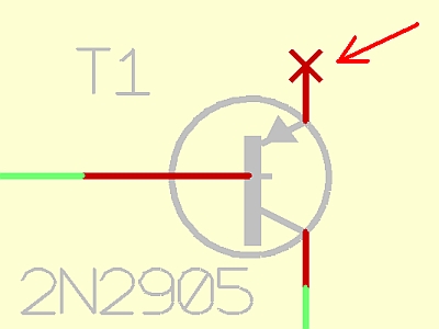
Place a pin when creating a schematic symbol
You can reach this mode...
by [1] or
by "Place Pin" in menu "Elements" or
by the icon ![]() .
.
Leave this mode...
by [ESC] or M12
What you can do...
You can place free pins with M1 clicks or by pressing [1] in pointer mode. Free pins are only used when defining new symbols which shall be saved as a component into a library. The pin numbers are incremented automatically. Press [o] (for pin options). Place the ultimate pin by [Return] or [Esc]. It is possible to change the pin number, the form and the function of the pins by pressing M11 in connection mode or with [o] for options. The following Options dialog shows some info about the component - and signal assignment. Other entries have the following meaning (release button ![]() in the pointer toolbar before doubleclicking a pin):
in the pointer toolbar before doubleclicking a pin):
Pin Options
The pin options dialog opens when pressing key [o] after selecting the "Place pin" mode from schematic menu "Elements". It is meant for defining a pin's properties for now and future placements. These placements are meant only for the creation of a new schematic symbol. All other pins you will import to the schematic as part of existing symbols through the component database. Even if a component has only one pin and one pad (C1x1)
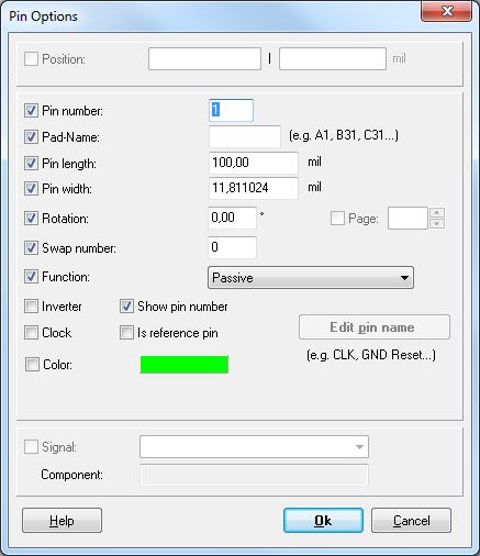
Pin number: The connection between the pin in the schematic and a pad in the package is this number. One of the most important informations a pin carries is the Pin number. Pin names are not regarded.
Pad names like A1-A20 and B1-B20 and C1-C20 are not regarded.
Pin length and width: Represent the hugeness of the red line element.
Rotation: Degree of rotation around the connection cross
Swap number: Pins within the same symbol or gate and with the same Swap number greater than zero can be swapped with this pin.
Function: Defines the function of the pin. Select from the following:
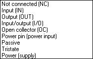
Not connected (NC): Pin is not connected (not used)
Input (IN): Pure Input
Output (OUT): Pure Output
Input/output (I/O): Changing input and output
Open Collector (OC): open collector output (open drain)
Power pin (Power input): Power supply of a component
Passiv: Pin of a passive element or function not clearly defined
3 States(Tristate): Output, which can achieve high-Ohm-impedance
Power (supply): Power supply of a PCB e.g. a connector supplying power to the PCB. Or the output of a voltage controller (e.g. 7805) which supplies others
Power pin means that this is a pin that needs power.
Power (supply) means that this pin gives power. Normally a connector pin is set to Power (supply). Power comes through this pin onto the PCB. Also pin 2 of a 7805 is a power supply pin. It supplies the other ICs with power. Their Power pins are consumer pins.
Inverter: The pin gets an inverter point.
Clock: A little arrow shows that this pin is a clock input.
Show pin number: Shall the pin number be visible? Useless for resistors, useful for ICs.
Is reference pin: If this box is checked, the pin is not representing a pad in PCB but is a signal reference pin such as used for ground symbols. This box shall only be used, when creating reference symbols.
Color: Define color of a pin independently of predefined color. Is color white (R=255, G=255, B=255) chosen, the predefined standard-color is used. If you wish color white although, you need minimal offset from the above mentioned RGB characters (just one point fits).
Edit pin name: The dialog for the pin name will be opened.
Change Pins
The Change pins dialog opens after M11 ohn a pin with the intension to change it. The dialog looks similar to the "Options" dialog but the entries refer only to this singular editing action.
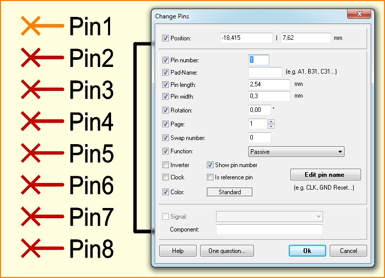
Position: Shows absolute coordinates.
Other functions as above.
A name is generated while creating a pin. This name can be selected separately to be renamed or moved. If you need for the logic of the circuit only the name of the pin but not the pin number please change the name and delete it with M1 and [Delete]. It will remain invisible.
Pin Swap
You can reach this mode...
by "Pin Swap" or in menu "Actions" or
by the tools ![]() .
.
Leave this mode...
by [ESC] or M12
What you can do...
Click the two pins or pads of the same symbol subsequently with M1. Both pins have to have the same non-zero swap number. In the schematic only the two pin numbers are exchanged. In the PCB the connected tracks are dragged along like rubber tracks. Caution: Short cuts are possible.
Pin Name
The Pin Name is the Text concerning a connection pin in the schematic showing its function e.g. GND or CLK or RES. Contrarily to the pin number it is a real individual data element in TARGET 3001!. It is placed or edited by a double click M11 on the Pin in question. The opening dialog is named: "Change Pins", see above. In this dialog please find button "Edit pin name" used to open the following dialog:
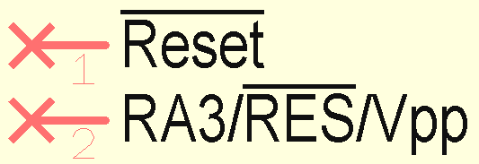
The pin name can also have an overbar. The pin name in the editor starts with a vertical bar (tube) then |. For example |Reset. The complete pin name has an overbar then. The overbar can also start within the pin name or end there: RA3/|RES|/Vpp. In the middle of the pin name has the word RES an overbar. Only one overbar can be used within a pin name.
Don't mix up Pin name and Pad name which is a alphanumerical naming of pads arranged like a matrix e.g. in BGAs or connectors (A1, A2, ... B1, B2, ... B31). Thus a Pin additionally to its Pin name can have an alphanumerical Pad name which will be displayed in schematic and layout instead of the Pin/Pad number. The Pin number nevertheless internally is kept as the internal link between pin and pad.
Anschlussnamen als Text bearbeiten
Diese Option findet sich im Schaltplanmenü "Bauteile". Zweck ist die Bearbeitung der Texte der Anschlusspins in einem Texteditor, der auch den Inhalt Ihrer Windows-Zwischenablage aufnehmen kann. Dadurch ist es sehr leicht, eine Vielzahl von Pins in einem Arbeitsgang zu beschriften.
Freie Pins beschriften
Wenn Sie ein neues Schaltplansymbol zeichnen, könnten Sie so vorgehen, dass Sie zunächst die Anzahl der erforderlichen Pins an eine freie Stelle eines beliebigen oder leeren Schaltplans absetzen. Öffnen Sie jetzt die Menüoption "Anschlussname als Text bearbeiten" im Schaltplanmenü "Bauteile".
Bild: AnschlussnamenText1_d.jpg
Bild: Beliebig 10 freie Pins gesetzt und den Dialog geöffnet
Im sich öffnenden Dialog wird in der Spalte links die jeweilige Pinnummer aufgeführt und im Textfeld rechts daneben werden die Pin-Namen sufgelistet, die Sie nun auf einen Streich editieren können.
TIPP: nehmen Sie die Pin-Namen aus Ihrem Datenblatt-PDF in die Zwischenablage und setzen Sie sie hier in diesem Textfeld ab. Verschieben Sie sie nun einfach zur gewünschten Pin-Nummer - fertig.
Die Pins eines im Schaltplan befindlichen Symbols beschriften oder umbenennen
Markieren Sie ein im Schaltplan befindliches Symbol als ganzes und wählen Sie die Option "Anschlussnamen als Text bearbeiten" im Menü "Bauteile". Im sich öffnenden Dialog sind alle Pins des Bauteils aufgereiht, so dass Sie direkt die Namen editieren können. Auch hier können sie die Zwischenablage benutzen.
Bild: AnschlussnamenText2_d.jpg
Bild: Die Pin-Namen eines bestehenden Bauteils editieren
Unsichtbare Namen sichtbar schalten: Sollten Sie Pin-Namen durch "Entfernen" gelöscht haben, können Sie ihn hier zur sinnvollen Bearbeitung wieder sichtbar schalten.
