FAQ: Schematic
Multiplying schematic parts and multiplying the layouts also
My schematic contains several modular circuits all identical to each other. When in PCB mode, if one circuit is drawn, how can it be copied using the numbering from the schematic? Just using copy or duplicate, forces the next corresponding component numbers after the last one in the schematic. In my project I have four sub modules in the schematic, I have laid out one in PCB mode, and now wish to duplicate another 3 to match the schematic without completely manually re drawing each. How can I do that?
Please draw one part of the schematic and do the layout. Now copy it within the schematic once. Switch over to the layout and copy it also once. Return to the schematic and copy it a third time, go to the layout and also copy it a third time. Go back to the schematic and copy it the fourth time, go to the layout and copy it a forth time. If you are doing it close in time to each other, you will have no struggles with the numbering.
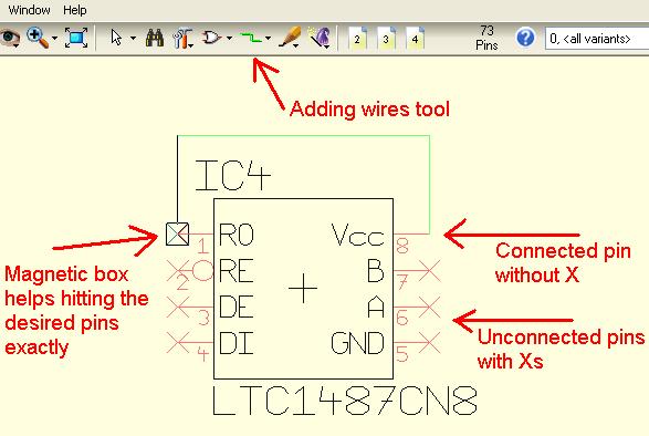
How can I add a signal wire to the schematic and connect to components reliably?
.
Clicking on a component selects only an internal part of it. It should select the whole thing. How can I do that?
You can use the handle cross to select the component completely. Also you can set an option to have exactly your desired behaviour: In menu "File / Settings-Options" the dialog "TARGET preferences and options" has a toggle: "Catch component - always complete".
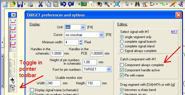
Select component always complete
It is one of TARGET's great advantages being able to edit a component after it is inserted:
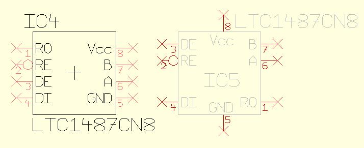
Adapting a schematics symbol to the needs of the circuit for better readability
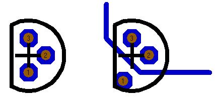
Adapting a package symbol to the needs of routing
Nothing is changed in the libraries to avoid confusion with several symbols with similar names, all of the same component.
Darken/thicken Pin names
I cannot darken (thicken) the pin names and numbers on the printed schematic. I have tried 'Settings (project)', and can change the appearance on the PC screen, but not the printed copy.
Please have a look at menu "Window/SettingsOptions"and use the entry "Height of Pin numbers in schematic...":
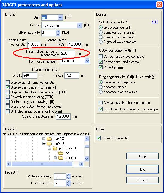
.
Junctions/knots in the schematic appear too thin. How can I preset the diameter of the knots in general to e.g. 0,5 mm?
- Open a new project and press key [o] for "options".
- Set the options as desired on the new schematic page. (e.g. junction width, track width, etc.).
- In menu "File" save the project as Template.T3001. When starting a new project, all settings will be used from this project template file. See also Default.
I edited an aperture list. Which meaning have the abbv´s FK, FQ, etc..?
- FK (Fahr-Kreis): circular traction apertures for traces, triangles, circles (Draw)
- FQ (Fahr-Quadrat): square traction aperture for rectangles (Square)
- BE (Blitz-Ellipse): ellipt./round flash apertures for soldering pads (evtl. Round or Oblong)
- BA (Blitz-Achteck): octagonal flash apertures for soldering pads (Octagon or evtl. Oblong)
- BR (Blitz-Rechteck): rectangular flash apertures for soldering pads (Oblong)
- BO (Blitz-Oval): oval flash apertures for soldering pads (Oblong)
- BB (Blitz-Bohr): symbol meaning a drillhole
