Layout
  |
 Easy layout drawing |
A layout is the binding construction plan of a PCB. In TARGET 3001! it can be edited with or without a schematic.
The expressions layout und PCB or PCB view are often used synonymous in TARGET 3001!, because the same module is meant. The layout is edited in the PCB view. For reaching the PCB layout view in TARGET 3001! click this icon: ![]()
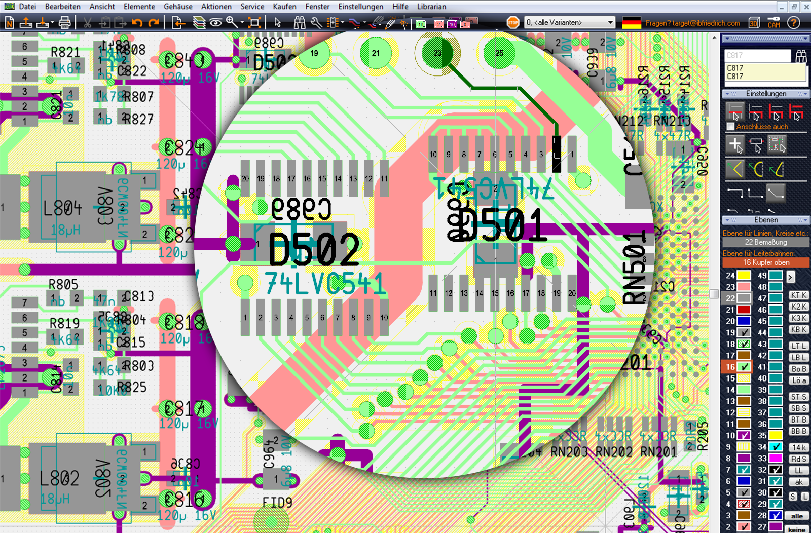
This icon appears in any schematic view. You also might use the [F3] key or the [Shift]+[F3] key. A simple PCB layout might look like this:
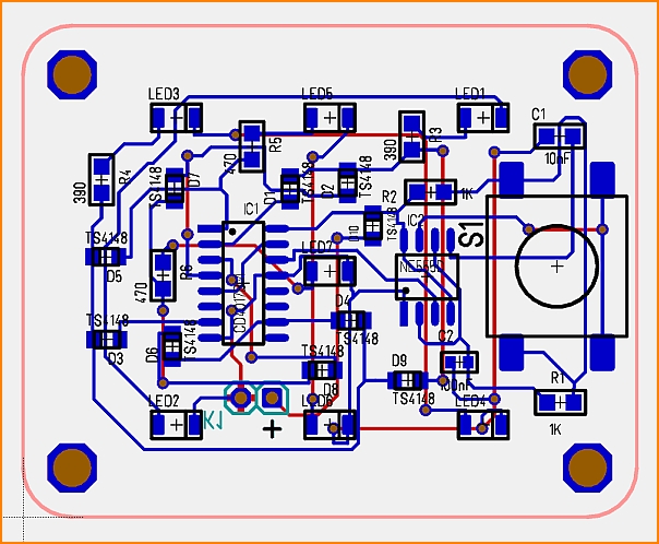
By the use of the default settings you see:
the PCB outline (pink),
the soldering pads (footprints, landmarks) of the components (blue),
the padnumbers (black),
the drillholes (brown),
the elements of the copper top side (blue),
the elements of the copper bottom side (red),
the position print with package outlines and component names and values (black)
