Solder a wire to a board
How to solder a wire to your board?
By placing a one pole connector! How to do that?
With a counterpart in the schematic
Select a single pole connector from the component data base. Search in the TARGET 3001!- component data base ![]() for 1 pole. Select from the row of female sockets the C1x01_SOCKET. You will get the following image (sure it would be appropriate to insert a male 1 pole pin header as well):
for 1 pole. Select from the row of female sockets the C1x01_SOCKET. You will get the following image (sure it would be appropriate to insert a male 1 pole pin header as well):
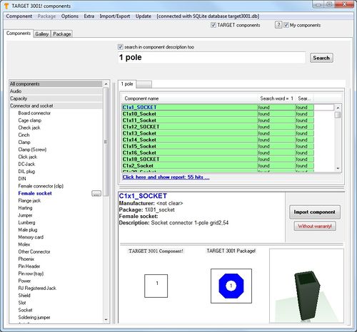
Image: The component browser with suitable match.
Import the componennt to the schematic. Here you get a single pin which you would drop to any place of your schematic and connect it. Now switch over to the layout view. ![]() and place the pad.
and place the pad.
With a drill hole (THT)
If a pad expects a wire/lead from a part (THT Pad, Through Hole Technique, plated through) it will appear in this shape to your layout:
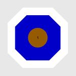
image: A soldering pad meant for mounting a wired pad.
If you fade out the board material the soldering pad would look this way:

Image: a soldering pad, meant for mounting, soldering a wired lead.
The form and the look of the pad can freely be edited, especially the copper height and width as well as the drill hole diameter. Later any current leading connector can be soldered here, a wire or any other contacting element.
Double click M11 on a soldering pad in the layout opens the dialog for edition. First release eventually this button: ![]()
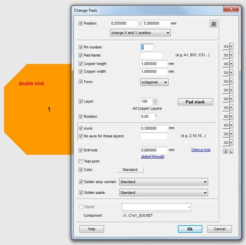
Image: Double click on a soldering pad opens the dialog for edition.
Without a drill hole SMD
In order to make a THT pad a SMD one, take away its drilling and set the layer from 100 either to 16, copper top or 2, copper bottom.
In the dialog above named "Change soldering pad" simpla set the drill hole dialmeter to zero . This means: "No drilling". Now set the layer from 100, AllCopperLayers to 16, copper top or 2, copper bottom. So you get a SMD pad at the desired copper side.

Image: A little more copper width than height, Layer=16, drill hole diameter=0mm
Result:
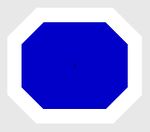
Image: A little more copper width than hight. Layer=16, drill hole diameter=0mm
In der 3D view it looks that way:
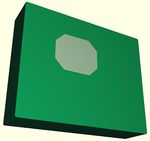
Image: A SMD soldering pad is just a plated copper area on the PCB.
Without the board you would see just an octagonal square in gray. Not quite exciting but exactly what we desired to have.
Without a counterpart in the schematic
In a Project without schematic simply select the package:
1X01_socket
Place the soldering pad at any place in your design. M11 allows edition.
Create a simple soldering area on "copper top" for example
Select a filled rectangle in the drawing functions (the pencil icon). The cursor shape changes. Hover the mouse to layer 16 at the sidebar to the right and do a right click M2. Now layer 16 is active for drawing, highlighted red. Now place your rectangle to the canvas. It appears blue in filled shape. This area will be constructed later as a little copper area on copper top. Kopy and paste this area again on layer 18 solderstop top so that this little pad later remains free from solderstop varnish. If all layers are faded in later, the pad appears green. All green elements are free from solderstop varnish thus solderable.
alias: soldering pad footprint, single pole, one pole, contact, simple connection
