Polygonal pads
Create custom shaped polygonal pads
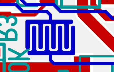
Polygonal pads are often required for SMD-LEDs, heatsink pads, tactile switches and so on. Click M11 on any pad in order to edit it. The Change Pads dialog opens...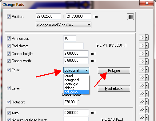
In the dialog for pad edition there is a pad function:polygonal and the button [Polygon]. If you push it, the polygon editor starts.
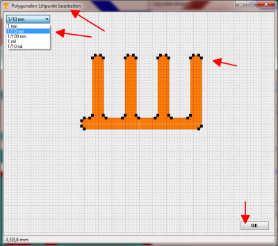
In the polygon editor first set the grid to an appropriate size. Now move the existing black points (anchors, vertices) by drag&drop M1H. Please note the coordinates in the status line bottom of the dialog. In order to create new points, click M1 close to an edge (inner or outer) into free space. If you click M2 on an anchor a dialog appears allowing edition. Finally press [OK] to accept the polygon as new pad shape.
If the canvas of 10mm x 10mm appears to small, pleae use the box top right in order to enlarge the drawing area to max. 10cm x 10cm. Center of the canvas always is THE anchor for the pad as a whole. A drillhole will be centered there as well. The drollhole diameter defines the existence and the performance of a drillhole. Drillhole diameter =0 means: No Drillhole.
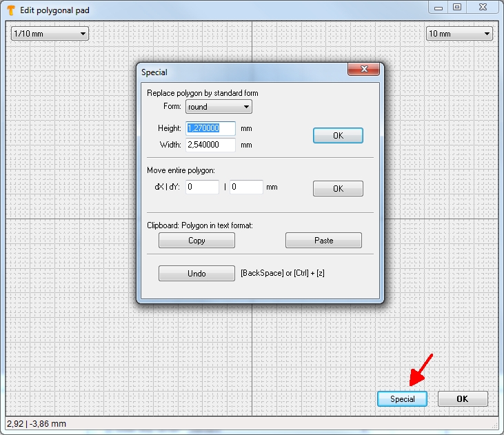
Image: With version V18 there are some additional options to specify the polygonal pad.
A user asks:
For a chip I need pads having the shape like the image. How can I do that?
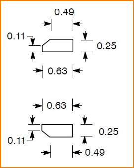
Image 1: Measurements from the data sheet
Solution:
Drop any soldering pad to the layout. A double click on it opens the dialog "Change Pads". Now give the pad a rectangular shape according to the data sheet having a width of 0.63mm and a hight of 0.25mm. Set: Layer 16, copper top and Drill hole =0mm (which means no drill hole). Press OK and the pad appears in this shape. Again a double click on it and now select pad "Form": Polygonal and press button "Polygon". You get asked whether to derive the coming polygon from a former form which you confirm by "Yes" . Now your blank gets taken over to the editor. You can zoom in and out with the mouse wheel. A 2mm is optically OK here. The little black touchpad (vertex) top left of the image now can be clicked M2, in order to enter its coordinates manually.
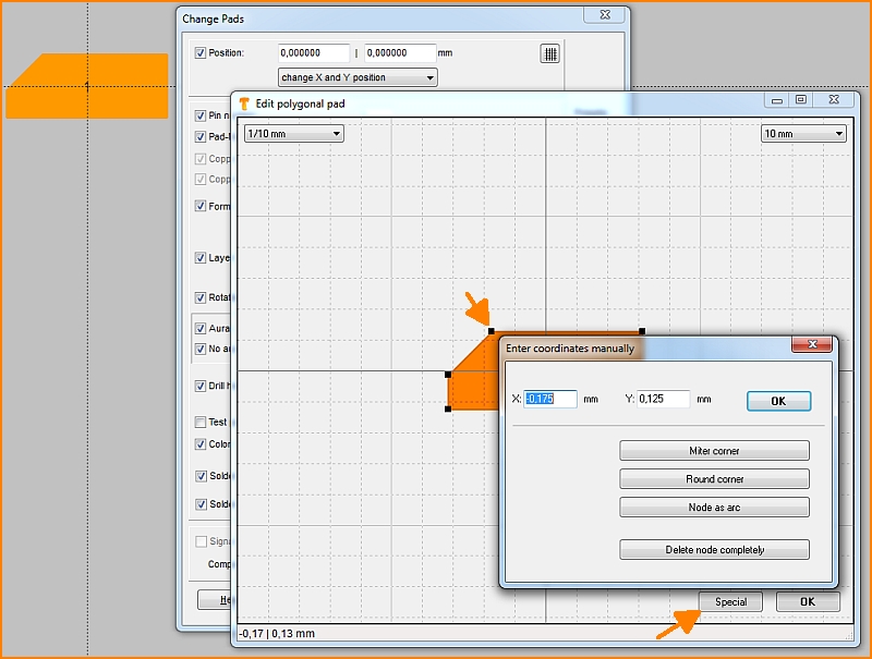
Image 2: Edit a polygonal soldering pad. Remark: The image had been created after the pad had been generated (it is the reason why the resulting pad (yellow, top left) already has the desired form.)
Create a further vertex by a click on the desired spot. The new vertex slips to the nearest spot on the grid and can now be edited as described above. The button "Special" beside the OK button gives opportunity to enter the following text list (see arrow in image below):
Polygon [nm]
315000|125000
-175000|125000
-315000|-15000
-315000|-125000
315000|-125000
You can create the second pad by copy and paste of the first one ([Ctrl]+[c] and [Ctrl]+[v]) and then mirroring it by its horizontal axis. Do this also in dialog "Special":
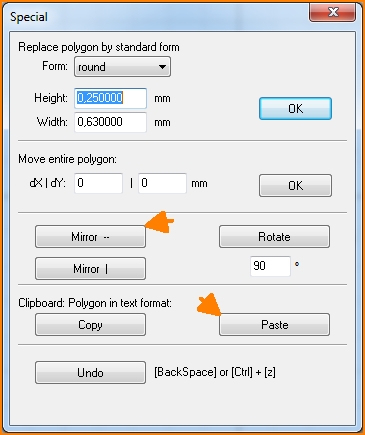
Image 3: Mirror a polygonal soldering pad by its horizontal axis.
Result:
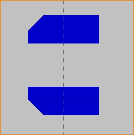
Image 4: Two polygonal soldering pads according to data sheet while the distance of both is not defined by the datasheet excerpt.
