EMC Check
General
The increasing expectations on the immunity and sensibility for disturbance with electronic device thus regarding their PCB is an important topic. Using the TARGET EMC tool, the PCB can be checked in terms of EMC while designing it. Also analyzing the auto immunity of a PCB and its influences it can take by emitting distortion can be analyzed. The chapter is completed with hints and advice for designing an EMC optimized PCB.
Introduction
To make sure that electronic device are able to work with their surroundings satisfactory, lots of rules and regulations do exist we have to stick to. On January 1st 1996 the referring act (EU-law 89/336/EWG), binding in Europe, statutes new conditions regarding electronic sets brought into circulation first after the mentioned date. That means any electronic set on the one hand must work error free in a electromagnetic disturbed surrounding and on the other hand must not disturb other equipments. As a consequence a conventional development of electronic device needs to be expanded by EMC analysis for to avoid later (expensive) corrections. For a developer it would be most comfortable if the design package he uses would guide him to an immune PCB.
The most important construction element of a PCB is the signal track. It connects signal source and signal sink. Its performance has significant influence on the EM properties of the circuit. The purpose of EMC is the generation of an unweakened and disturbance free transmission of the signal from sender to recipient. This aim always can be reached only approximately.
The following calculation methods have been considered for to recognize misleading influences on signal tracks:
Calculation of galvanic coupling: Galvanic couplings happen, if a circuit (source) uses the same return line. It mainly occurs on ground lines or power tracks.
Calculation of inductive coupling: The cause of inductive disturbing coupling is the change of the magnetic flow, which the circuit of the disturbing source inflicts into the circuits area of the disturbance sink. So those signals are interesting on which significant changes of flow in short time happen or those leading flow in high frequency.
Calculation of capacitive coupling: Capacitive couplings occur between two circuits whose signals show different potentials. High frequency or low rise times respectively have influence.
Calculation of the coupling factor: The coupling factor rates inductive and capacitive coupling together.
Calculation of the radiation coupling: In high clocking semiconductor circuits signal loops are the reason for radiation coupling. Because of relatively high flow steps in the conductors dynamic magnetic fields are generated. The individual current loops have an antenna-effect with the characteristic of a magnetic dipole. The amount of the resulting magnetic and electric disturbance field strength depends on the rise time, the clock frequency, the current of the loop and the corresponding loop area.
Calculation of the maximum track length: A signal track may not have any length. The signal frequencies and the rise times only allow a maximum length. Is it passed, disturbances can occur e.g. reflections. The original signal could be modified and an error could be the result.
Handling of the EMC Analysis tool
Input Dialog
You can start the EMC tool at any time. It makes sense starting it after all signal tracks have properly been routed.
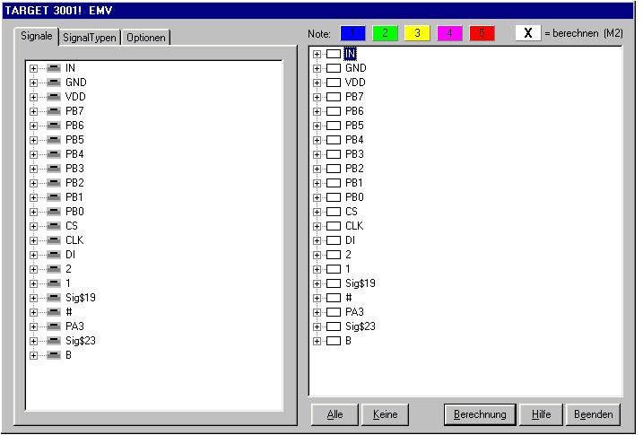
Start this tool in layout view in menu "Actions" and "Start EMC check..." or choose the button shown above under the wizard. The complete handling is managed in one dialog. The Windows 95-Tree-View-Technique has been used you may know from the Explorer.
In the dialog on the left you see all signals routed in PCB view listed. Afterwards the signals are provided with different properties. In the dialog on the right you choose the check routine and the signals to be checked. Analysis and evaluation are displayed colored.
How to proceed
All settings and allocations are now described like a list:
1) Edit signal list
In the left part of the dialog the complete signal list of the already wired signals is shown. Click on {Plus.bmp} and all possible properties of a signal are listed.
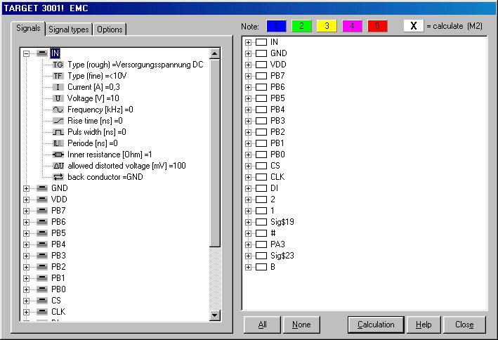
M11 on an entry opens the dialog "Set the EMC properties of a Signal":
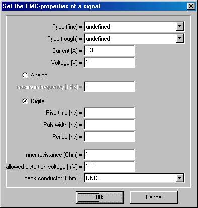
First allocate the requested properties to the signals. Type (rough) means classification "rough", Type (fine) means classification "fine". For example rough = digital signal TTL, fine = technology HCT. By the entry "back conductor" (= return line) you can set the reference signal of a disturber. This entry is important (fundamental) for calculation of the coupling factor, the capacitive and the inductive coupling. Without a definition of those properties a sense making EMC analysis is not possible.
2) Edit properties and set new
Click on register "SignalTypes". First all of the existing properties are listed. By M11 the properties can be edited. For avoiding the case that a signal can not be provided with standard properties press button "New" for to set individual properties. First choose a suitable name for the property. Afterwards the signal type has to be defined. If you highlight "analog", please set the frequency at "technical data". Otherwise (when choosing "digital" type) the risetime and the pulsewidth must be entered. Furthermore the values for current and voltage are important for the EMC calculations later. They need to be set.
This point 2) can be ignored if you don't need to define new signal properties.
3) Set Options
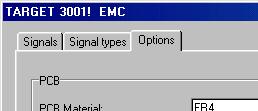
Click on register "Options". Please enter data regarding the board material: kind of material (e.g. FR4) dielectric constant (is defined by the kind of material) thickness of material (e.g. 1,5 mm = 1500 µm) copper coating (e.g. 35 m)
All other geometrical data are calculated by TARGET (track length, track width, number of layers).
4) Select analyzing modes
In the listing to the right all signals are shown. Highlight the signals you wish to check regarding EMC as follows:
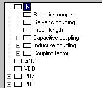
Select by M11 a signal to be checked (in our example it's the signal IN). This signal is used as a "disturber signal". The tree view suggests automatically all opportunities of calculation.
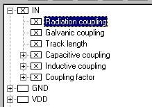
M2 on signal IN prepares all analyzing modes for the calculation later on. You can individually select by M2 only those which are of interest for the check. The return line can not be chosen as a disturbed because it had been defined with the signal list.
5) Start calculation
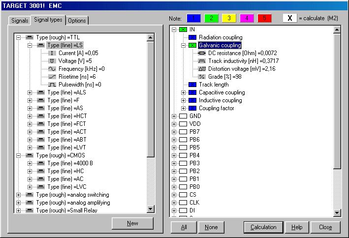
Click on button "Calculation". As a graphical analysis the signals are shown in a colored rating ("Note") from 1 to 5.
Meaning of the colors:
blue: Note 1: (rating: 100%)
green: Note 2: (rating: 90% - 99%)
yellow: Note 3: (rating: 50% - 89%)
purple: Note 4: (rating: 1% - 49%)
red: Note 5: (rating: 0%)
The calculation results are shown in a list:
Using the following formula the analysis of the percentual rating is explained:
Regarding the length of the track is:
Percentage=

Regarding all other calculations is:
Percentage=

lsignal = length of signal (track) lzul = allowed length of signal (track) Ustör = disturbance voltage Uzul = allowed voltage of the signal
The result of the radiation coupling is shown in a graphic. The calculated results are compared with the limits following
VDE 0871/B and EN55022. By M11 on radiation coupling the following picture appears.
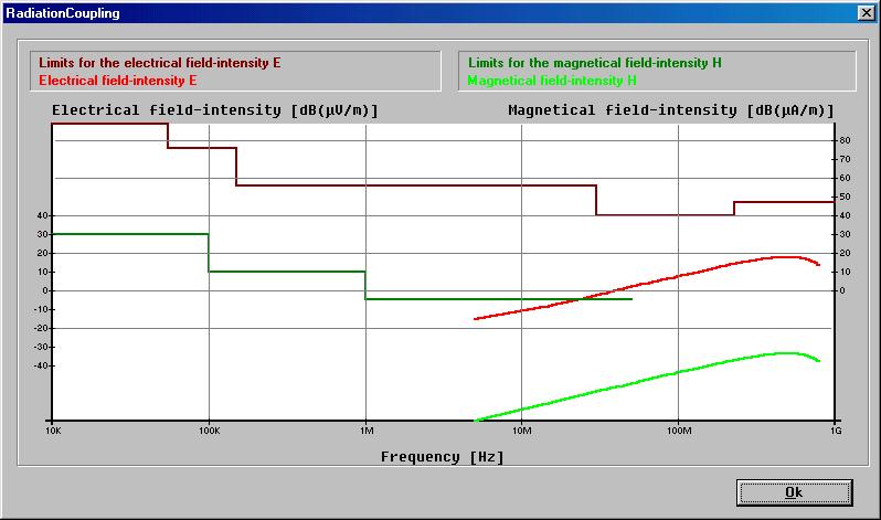
If the calculated values grow beyond the limits, the critical area is shown yellow (in the listing the box is shown red).
The abscissa shows the frequencies in logarithmic scale, the ordinates on the right and on the left refer to the electrical resp. magnetic field strength. The brown line shows the defined limit line regarding the electrical field strength. The calculated curve of the electrical disturbing field strength is red. The green line shows the defined limit line regarding the magnetic field strength. The calculated curve of the magnetic disturbing field strength is green. In an ideal case the calculated curves show below or upon the limit line. In other cases countermeasures need to be done - e.g. reduction of the loop area.
Kinds of coupling
Calculation of the coupling factor In the tree view the calculated results are shown after the button "Calculation" was clicked. Calculated are the coupling factor between the disturbing and the disturbed signal (taken from the inductive and capacitive track stressings) and the wave resistance of the arrangement. Moreover an EMC rating is made. TARGET calculates a percentage which informs the user whether a critical value is reached.
Calculation of the inductive coupling The results regarding the inductive coupling between the disturbing and the disturbed signal are shown. The following results are displayed: Counter inductivity of the coupling arrangement and the disturbance voltage, which is transferred from the disturbing signal to the disturbed signal by inductive coupling. Also an EMC rating is made, showing whether both signals perform in an EMC critical range.
Calculation of the capacitive coupling The following results are calculated and shown: coupling capacity between disturber and disturbed, disturbed signal's current, caused by capacitive coupling of the disturbed signal and the disturbing voltage over the inner resistance of the disturbed signal, caused by the cross coupled disturbing current. Also an EMC rating is made, showing whether both signals perform in an EMC critical range.
Calculation of the galvanic coupling After pressing button "Calculation" the following results appear: DC-resistance of the signal, line inductivity of the signal and the disturbing voltage upon the signal, caused by galvanic coupling on this
Calculation of the allowed track length The maximum length is compared to the real length. The user can see whether reflections to the track (line) could occur.
Calculation of the radiation coupling Please see chapter 9.1.{9.1 Introduction}
Prevention of EMC disturbance
The electromagnetic compatibility of a device needs to be made sure in three aspects:
- no external disturbances
- no internal disturbances
- it must not act as a source of disturbance
For reaching those aims a developer has to follow several rules. The most important points and the corresponding explanations are shown in the following chapters. If you follow those advice you won't face severe EMC-problems.
Wiring of reference potential (GND)
It is obvious to minimize galvanic coupling by avoiding a shared use of signal tracks. This could be reached by placing completely separated return lines (star shaped ground). Because of the increasing amount of tracks and their density the capacitive and inductive couplings will increase. The separation of the shared tracks and the reduction of the coupling impedances is a practicable measurement.
The lower the track impedance and the generating current resp. change in current is, the lower is the disturbance voltage regarding galvanic coupling. The current is defined by the need of it thus not a free disposable value. As a measurement for oppressing a disturbance coupling we only can choose the reduction of the track impedance. For its decrease the following aspects may be considerable:
- short tracks (lowers the ohm- and inductive proportions as well as the skin-effect; having effect on the entire frequency range)
- big track diameter (lowers the ohm- proportion, is especially effective at DC and low frequencies)
- big track surface (lowers the skin effect, effective at high frequencies resp. quick current changes e.g. several thin tracks besides each other)
- small area of current loop (lowers auto inductivity radiation surface)
The highest disturbance voltages in galvanic coupling arise because of voltage falls when quick changing current. The ohm- proportion has influence because of the skin effect. Also the auto inductivity of the track is effective. For the auto inductivity changes only few regarding to the track diameter and as it can be modified only few on the board , we concentrate on the most effective measurements: shortening the track lengths and arrange them in respect of their use.
Star-shaped structure of reference conductors
The impedance may not be ignored when wiring the reference potential. In the worst case the related potential can show different values on different points. This case for instance is made clear in the following picture showing a substitute with an elementary row ground structure:

Circuit of several steps in an "elementary row ground structure".
In a circuit of this structure every step controls only the following step and is controlled itself only by its preceding step.The impedance Zgi of the track from the steps ground star point to the systems potential compensation (point A to E with impedances Zki,(i+1) ) couples entry- and exit circuit of this step. Whether this effects disturbing can be defined without recognizing the rest of the circuit because a disturbance is caused only within this step. On the related potential resp. ground between the steps i and i+1 (impedance Zki,(i+1) ) only the current between both step flows. Also the ground input and exit clamps of the circuit are flown through by the related input and exit current.
At the impedances Zki,(i+1) of the ground parts between the steps decreases of voltage arise caused by each of the signal currents.They add up to the voltage UAE between entry and exit ground clamps. This fact remains without disturbing consequences as long as the clamps are not connected anyhow by other paths. Otherwise a ground loop is built up.
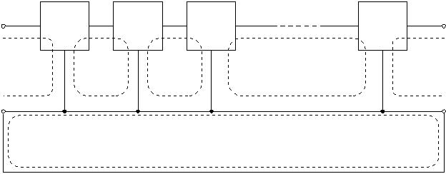
Ground loop on an "elementary row ground structure"
The signal currents not only flow back to the source by the related impedances Zki,(i+1), but also by the grounds of the other paths. But so all steps touched by this paths are coupled as the current analysis shows. The next picture shows the coupling of all steps in a parallel connection of ground within two circuits with "row ground structure".
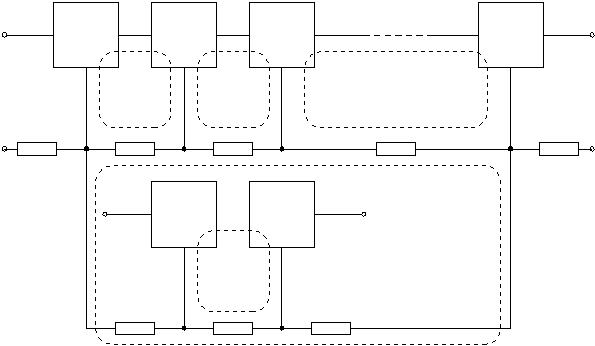
Ground loop out of two circuits with "row ground structure"
If the circuit is optimized the way that all Zki grow zero, a star structure of ground emerges. The ground connections of all steps meet in the "star center". As long tracks increase the related impedances Zgi, short tracks should be chosen.

The star structure eliminates the impedances of the potential compensation system between each of the steps.
Meshed tracking
If a star shaped structure is not effective because the signal tracks grow too long meshed tracking can be used. Also using this method a decrease of galvanic coupling can be reached. Here several parallel reference conductors are connected to each other like honey combs. They make up several closed track loops having shorter track lengths and lower impedances for signals flowing than in a star shaped arrangement.
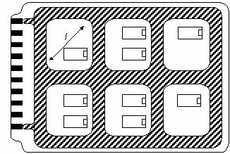
Have a look at the maximum width of the meshes. A current flow in them causes a radiation. It remains as low as its largest measurement l is. With decreasing l the radiation decreases quadratic so that in normal current flows no radiations of note arise.
Separation of signal and current referring conductors
A further option to avoid galvanic coupling is the separation of the reference flow conductors of signal leading circuits from those which have bigger needs of current. It can be divided in:
- signal reference flow conductors
- current reference flow conductors
Signal referring conductors are tracks not having stressed the reference potential regarding current (switch inputs). I. e. the sensible circuit areas as well as the reference potentials and the input supply of pre amplifiers. The current flow through those tracks amounts up to some mA.
Current referring conductors are tracks which often are stressed by higher (return) flows. Those target the power supply (OV) as well as the return flow of the initial current signal.
This division is arbitrary. Its aim is to divide between rather disturbance generating and rather disturbance sensible tracks. If the reference tracks can be divided to both groups one will have a system which is nearly insensible against galvanic coupling. This is important with systems consisting of a mix of digital and analog systems.
When wiring the reference potential (star structure) we can see, that the reference potential of the analog system had been separated from the digital one.
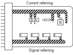
Wiring of signal tracks
For judging the EMC properties of signal transferring the whole circuit, i. e. the signal track as well as the return line has to be recognized. Humble structures show the current flow returning by the reference potential so we face an asymmetrical signal coupling. Most of the signal transferences have those structures. Asymmetrical arrangements have the currents returning by the same tracks and so inherit the danger of galvanic coupling. If immunity should be maximized the following aspects need to be recognized:
a nearly non disturbed reference potential must be offered to the signals. (Using a star-structure the galvanic coupling is reduced.) for reaching a low inductive coupling the whole current loop ( signal track and reference potential) must show a minimal area. This can be reached by: a short track (in general) a close arrangement of signal track and return line (see picture).
Following those rules also the disturbances going out from this circuit as a source are reduced.
for minimization of capacitive coupling the tracks and especially their parallel placement need to be short and the distances between them need to be big.
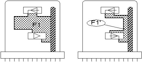
left: suboptimal because of big current loop area
right: favourable because of lowering the disturbance by reducing the current loop area.
A common transference of several signals a low coupling of signals should be considered. It can be reached for instance by placing a grounded current free track between signal leading tracks.
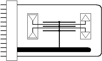
Lowering the capacitive disturbances by insertion of shielding tracks. This kind of tracking is suitable when routing multilayer PCB.
Wiring of supply tracks
Supply tracks can be divided into: DC supply (VCC) and return line (0V; common reference potential)
The problems placing power tracks are similar to those of the reference potential: The power supply of a component generates an decline of voltage within the power supply track which means a decline of power voltage. The galvanic disturbances influence the voltage leading tracks as well as the 0-Volt track (return line).
The 0V- supply track is the reference potential (GND). Take care of a low Ohm performance. Tracks should be short and broad.
Wiring of Voltage leading tracks
Because most of the circuits are more immune against variations of the supply voltage rather than against variations of the referring potential slight disturbing voltages effect less dramatic here than on the reference potential. Nevertheless big disturbing voltage can be the reason for disturbances.
For the reason of disturbing voltages is to be seen in voltage declines within the track impedances especially quick changes in current flow are harmful.
For lowering those disturbance voltage the same aspects can be recognized as already shown in chapter 9.3.1 (see picture).
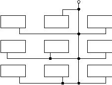
Arrangement of the power track with low coupling effects.
Components with big current needs should be placed close to the power source and the supply track to each of the component is short. Placing VCC and GND on the outer edge of the PCB also supports the decline of disturbance. Measurements regarding the placements of tracks don't need to be done following the same consequence as regarding the reference potential. Here we have the opportunity to buffer the required current using blocking capacitors - taking support by the reference potential.
Use of blocking capacitors
Between power voltage and the reference potential at any circuit (place of consumption) a capacity for buffering reasons is fixed (blocking capacitor). This capacity rises up to the supply voltage. If needed current (potential) can be delivered. So the power voltage can be kept within a calculable range if sudden potential demand occurs.
The consuming loop needs to show a low impedance for to let the potential flow from the capacitor quick enough (i. e. the buffering effect). The consuming loop consists of:
- the length of all connecting wires of the blocking capacitor
- the inner ways within the capacitors (including capacitance per unit length)
- the tracks from capacitor connection to consuming component
- the inner tracks within the shielded component
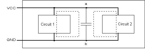
Elimination of disturbing influence by shifting the connecting star points
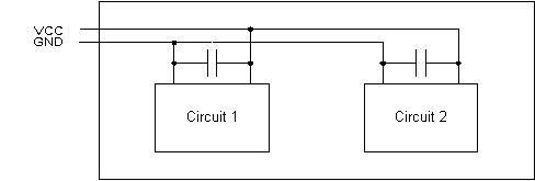
Favourable arrangement of blocking capacitors
The faster the signals are that means the faster the current nees rises the closer need the blocking capacitors be fixed to the component connections of VCC and GND. At high frequencies it depends on every mil of track length. The value of capacity should not grow too big because beyond the optimum value its effect declines. Blocking capacitors are also suitable for easing of Ohm caused voltage losses which arise at increased current needs of medium duration. Here higher capacity values need to be used which do not have to be fixed as close to the component.
Separation of digital and analog units
Unwelcome electromagnetic influences can appear in a circuit between analog and digital structures . It makes sense separating and decoupling analog from digital structures regarding the placement of components. That means not to lead digital signal tracks through analog signal systems and to place analog circuits to suitable areas on the PCB.

Left: Suboptimal placement of tracks Right: Favourable placement of tracks
It is important furnishing digital and analog systems on a board with separated referring potentials (GND).
Improvement of EMC properties
There are lots of measurements for improving EMC properties. First the disturbances (paths of coupling)need to be localized. Is the kind of disturbance known, individual measurements can be started.
Please note that about 95% of all disturbances are caused by the following kinds of coupling:
- common use of tracks (galvanic coupling)
- tracks too close to each other (capacitive and inductive coupling)
- field influence (radiation coupling)
Against generic EMC disturbances the following measurements can be helpful:
- reduce any disturbance on its source (e.g. shortening, drilling or shielding the tracks)
- interrupt the coupling paths of the disturbance (e. g. insert shielding metals, increase distances)
- save disturbing sinks (e. g. increase immunity, insert overvoltage arrester)
Advice regarding galvanic coupling
The reduction of galvanic coupling depends on the aspects:
- track length (as short as possible)
- track diameter (track width as wide as possible)
- the area of current loops (as small as possible)
Reduction of galvanic coupling on reference signals (GND): Placing tracks of reference signals please separate signal-reference signals (low need for current) from current reference signals (high need for current). Make sure that digital reference signals are separated from analog reference signals. Realize it by using multilayer PCB on which copper coated reference conductor areas resp. shielding areas are planned or realize it by using meshed tracking on double sided PCB. Meshed reference signal tracks hinder the track routing of the other signal tracks relatively few. It can be reached by dividing the meshing on to the lower and the upper copper layer. With normal track dimensions the measurements of the meshes will be realized at some inch, so that radiation to be mentioned will only occur at more than 300 MHz. Alternatively meshes can be used as shields around reference potential.
Reduction of galvanic coupling on power supply tracks: A high track width and short lengths are very important. Multilayer PCB could show a single layer solely as power supply. Supporting capacitors can be inserted if indifferencies in the supply tension occur. Return lines of power supply (0V) should be fixed to the reference potential (GND) on one allocation point. If we have several supply voltages with individual potential free 0V-connections for any track different connection points to the reference potential can be chosen.
Advice regarding inductive coupling
Low coupling in this respect is reached if signal tracks as well as reference potentials show small areas. Realize it by:
- placing short tracks and
- fixing them close to the return line.
Shield the signal tracks by placing GND tracks besides.
Advice regarding capacitive coupling
For minimization of capacitive disturbing coupling make sure that
- the tracks of disturber and disturbed are short
- their parallel tracking is short
- their spacing is wide
Parallel signal tracks lying on one layer, should use beside-tracks as return lines. So their area can be minimized. Here the return lines should run potential free. The signal tracks should run shielded by GND tracks besides.
Advice regarding radiation coupling
For to reduce the radiation of a signal the loop area (the area between disturbing signal and the signals reference signal) should be minimized. That means that besides the disturbing track the return line directly should be placed. If a reduction of the loop area can only be realized partly we have the opportunity shielding the radiation. Disturbing tracks can be shielded by metal sticks, coverings or little walls between (Al or Cu of 0,5 - 1mm).
Multilayers can have whole reference signal layers as shields. If there are not enough layers available the shielding can be realized by floating tracks. Especially those components need to be shielded, which are sensible on the one hand and on the other hand emit radiation relatively high. Often this is the case between digital and analog groups. Single components can be shielded by Al- caps (0.5 mm) touching the PCB. Transistors can use their own metal package being connected to GND. Simple functional blocks can be put into small metal boxes.
Advice regarding the coupling factor
In general: the longer the tracks of disturbed and disturbing signal are and the bigger their parallelism is, the stronger their influences will grow.
The coupling factor contains inductive and capacitive coupling as well as wave resistance. A reduction of the coupling factor can be read in chapters:
- Advice regarding inductive coupling
- Advice regarding capacitive coupling
- Advice regarding the length of signal tracks
Advice regarding the length of signal tracks
A track should be designed the same over the entire length and show no bends and forks. In most cases this cannot be realized. Please recognize the following aspects:
- short tracks
- no bends over 45°
- avoid change of layers (vias)
- tracks which are longer than the value the EMC analysis suggests and which can not be shortened, should be closed up using the same wave resistance like the track itself for to prevent reflections as far as possible.
- replace T-connections by star point shaped tracking
- enough spacing between digital and analog tracks. Place shielding tracks (GND)
Advice regarding blocking and supporting capacitors
Upon GND and supply track sudden changes in current flow (peaks) could arise, which cause disturbing voltage by inductivities within this tracks. Those disturbing voltages are the bigger, the longer the track is and the quicker the change in current flow is. To avoid it use supporting capacitors (ceramic) which are poor of inductivity. In the moment of peak they effect like a store and take over the peak. So it is kept out from further supply lines.
Supporting capacitors should be placed close to the IC's (at 1 to 10 nF). Every capacitor should be effective for 1 to 4 integrated circuits. To the exits of voltage controls supporting capacitors (about 10 F) are fixed in practice. Every PCB should have supporting capacitors of 1F on any power input. On tracks every 5 cm distance supporting capacitors of 0.1 F should be placed.
A clever arrangement of power supply tracks can help minimizing disturbances.(see advice regarding galvanic coupling)
Use the following typical capacities of supporting capacitors:
- for fast signals (f>80 MHz; risetime <5 ns ): 1000 pF
- for medium fast signals (f = 10 to 80 MHz; risetime = 5 to 40 ns ): 10 nF
- for slow signals (f < 10 MHz; risetime<40 ns): 33 nF to 0,1 F

