Multiple PCBs within one project
Within one project it is possible to divide a layout into several PCBs, see the following example: pic.t3001
The PCBs don't need to be identical. Apparently it is the signification of this tool that you are able to maintain as much different layouts within one project as you like. You are restricted only by the maximum board size of 47.24 in² (=1.2 m²) over all.
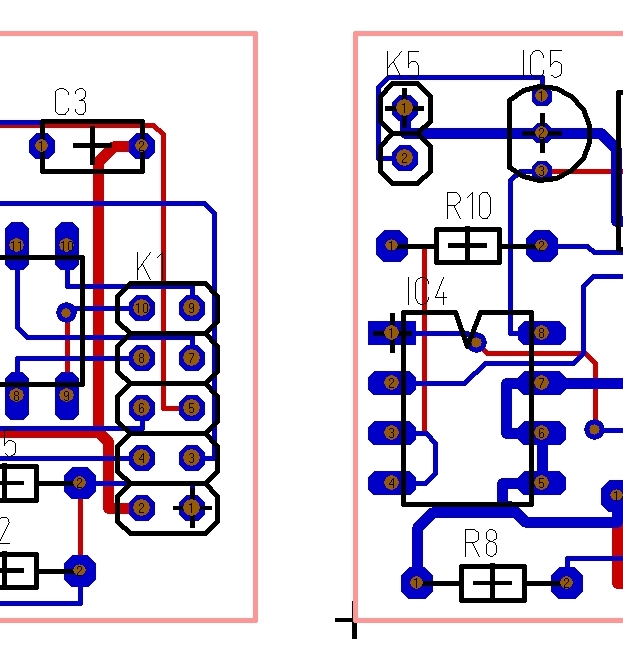
See these two layouts within one project which you'd like to treat separately:
First prepare the layer structure:
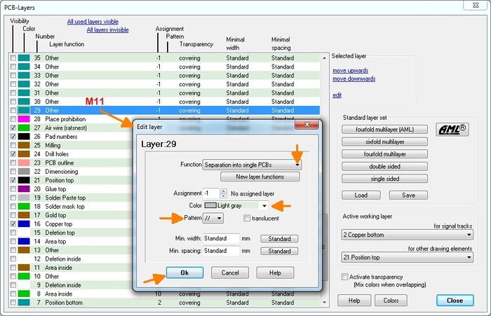
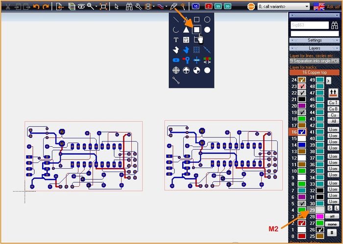
The individual PCBs now need to be covered by filled rectangles being drawn on layer: "Separation into single PCBs". In our case it's layer no. 29:
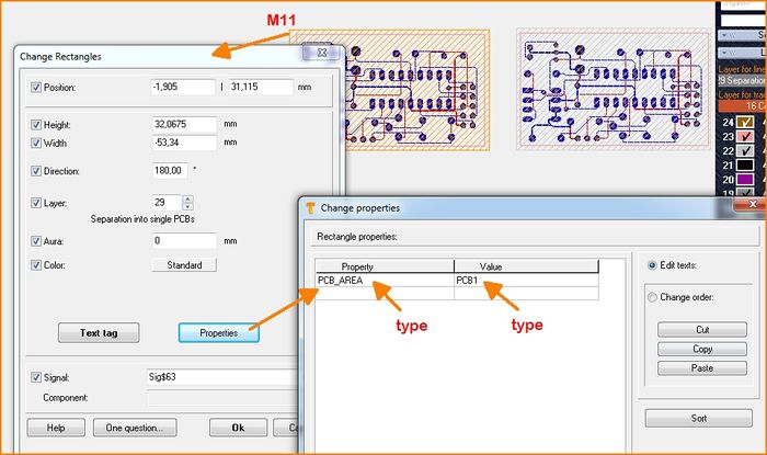
The next step is to assign it a "PCB_AREA" and to give it a name (e. g. "PCB 1"). Doubleclick rectangle, press [Properties], type the property "PCB_AREA" to the list at the left and enter name of the single PCB right beside.
Both the Gerber export...
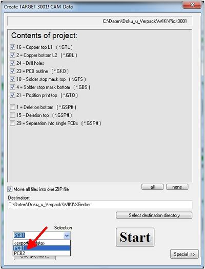
...and the generation of the Bill of Material allow choosing one of the PCBs:
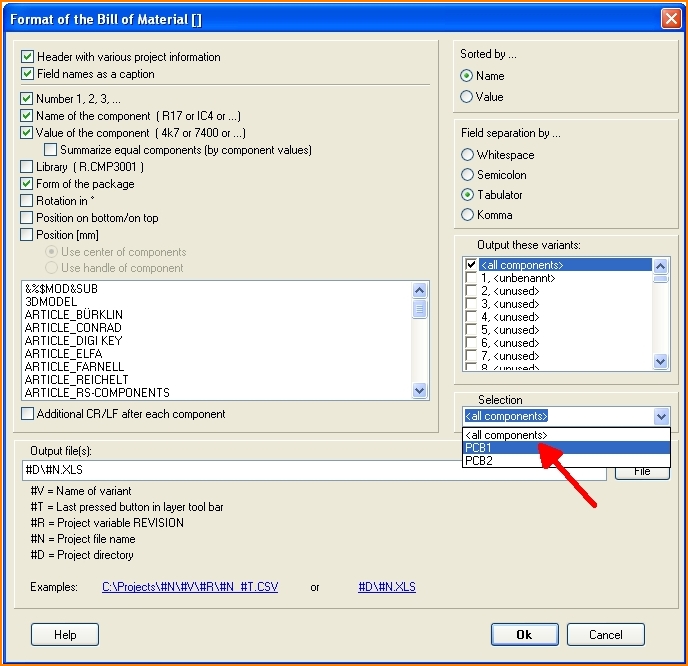
.
