Back view: Difference between revisions
Created page with "Klicken Sie auf dieses Symbol in der Sidebar, um die Platine zu wenden:<br><br> Button Rückansicht<br> (Bild 1: Button "Rückansicht" rechts in der Si..." |
No edit summary |
||
| (2 intermediate revisions by 2 users not shown) | |||
| Line 1: | Line 1: | ||
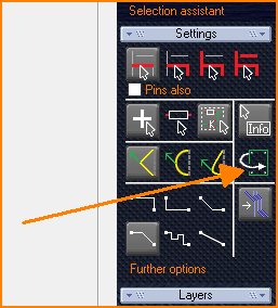
Click this icon in the sidebar to flip the board:<br><br> | |||
[[File:FlipPCB_EN.png|Button | [[File:FlipPCB_EN.png|Button Back view]]<br> | ||
( | (Image 1: Button "Back view" on the right in the sidebar)<br><br> | ||
You can also tap the [ | ] key (vertical bar / pipe) to change the view page. There is also a menu item for this in the "View" menu.<br><br> | |||
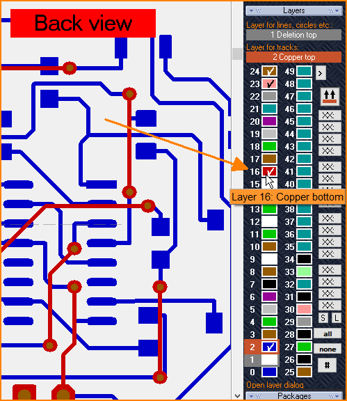
From the back side, you can now continue to edit the board as normal. Note that the layers at the bottom and at the top of the layer list are swapped: So the red layer "Copper bottom" is on 16 instead of 2 and so on:<br><br> | |||
[[File:FlipPCB2_EN.png| | [[File:FlipPCB2_EN.png|Layers swapped]]<br> | ||
( | (Image 2: Layers top / bottem are swapped)<br><br> | ||
Internal copper layers are also exchanged accordingly. The board is always flipped from right to left, i.e. always mirrored on the vertical axis. Before saving, the program automatically switches back to the normal view. The back view is additionally marked with a red banner in the upper left corner. From the V31 the feature " back view" is included.<br><br> | |||
aka: Flip the PCB, Back view, Flip the board | |||
[[ | [[fr:Vue arrière]][[de:Rückansicht]] | ||
Latest revision as of 20:13, 23 November 2021
Click this icon in the sidebar to flip the board:

(Image 1: Button "Back view" on the right in the sidebar)
You can also tap the [ | ] key (vertical bar / pipe) to change the view page. There is also a menu item for this in the "View" menu.
From the back side, you can now continue to edit the board as normal. Note that the layers at the bottom and at the top of the layer list are swapped: So the red layer "Copper bottom" is on 16 instead of 2 and so on:

(Image 2: Layers top / bottem are swapped)
Internal copper layers are also exchanged accordingly. The board is always flipped from right to left, i.e. always mirrored on the vertical axis. Before saving, the program automatically switches back to the normal view. The back view is additionally marked with a red banner in the upper left corner. From the V31 the feature " back view" is included.
aka: Flip the PCB, Back view, Flip the board

