FAQ: PCB Layout
Contents
- 1 I would like to have the component name show up on my silk screen,
- 2 How can I reduce the size of the component names and values on the layout screen?
- 3 Still airwires (ratsnest) in the layout
- 4 Groundplane: Thermal pads and rubout of signal islands
- 5 Milling tolerances and panel production
- 6 Is it possible create a gridded ground plane and a solid ground plane at same time on the same layer?
- 7 Pads: I want to have some millings for fastening/mounting a heatsink like oblong pads with oblong holes
- 8 Can I generate mass surfaces upon internal supply situations (multilayer)?
- 9 Tracks without soldermask
- 10 Is it possible to define cut-off areas in the layout for example to let autoplace only place the digital part of a circuit?
- 11 All SMD-components are automatically placed upon the lowest layer. How can I place them upon the top copper layer?
- 12 How do I create a PCB outline?
- 13 How can I set the track width in PCB mode once for the entire project?
- 14 How do I create a non rectangular ground plane?
- 15 How do I place " text ", e.g. the designation of the circuit board, into a ground area?
- 16 When placing component packages using the autoplacer, can the orientation be preselected (e.g. place all components horizontally in for later flow soldering)?
- 17 I have designed a PCB without a schematic and placed the air wires. How can I now remove placed air wires?
I would like to have the component name show up on my silk screen,
but I do not want to show the component values on the silkscreen because it will be too cluttered. Assuming I want to make a 2 layer board made by PCB-POOL, what is the best way to get rid of all the component value text from my PCB board? Can I just drag them outside the boundary of the physical board?
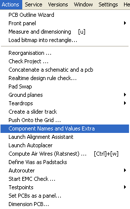
Please use option
This will lead to the fact that two separate layers are generated which each carry the name- or value data.
Now you can treat them separately and e.g. shift them to the silkscreen layer which by default is layer 21.
How can I reduce the size of the component names and values on the layout screen?
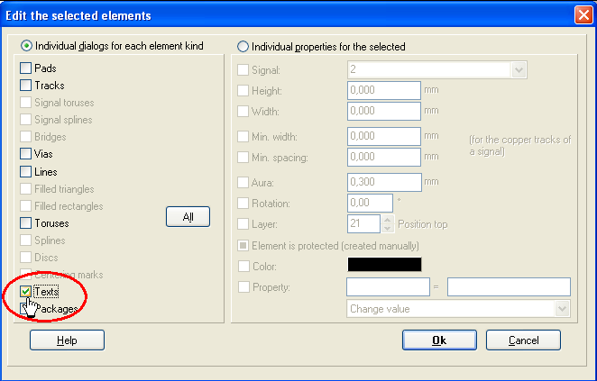
Highlight the complete layout by a Capture Window (= a highlighting square) now press keyboard key [e] (for edit). The flashing dialog allows selecting a certain kind of element:
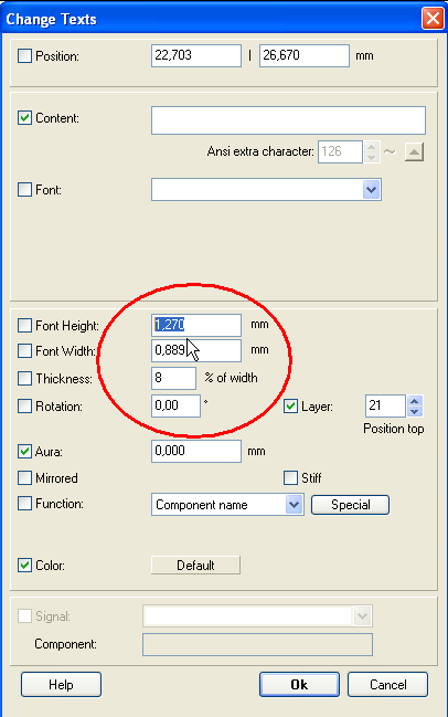
Press [Return] or OK for opening the individual dialog for entering an appropriate (reduced) value:
Still airwires (ratsnest) in the layout
Sometimes when I move a part, the air wire still shows it pointing to the old location even when there are no parts there on any layers. Checking the project says there is an error and it indicates that there is an unfinished trace even though the trace is completely finished. Even if I copy the Target file to a new one and completely delete the layout, sometimes the air wires are still there. Do you know how I can remove these strange air wires that should not be there?
We know about this behavior and have a little article regarding this topic
here.
Groundplane: Thermal pads and rubout of signal islands
Dear TARGET 3001! - Team,
when I click on thermal pad it does not work. My version is discover R12.6.
A thermal pad only works in a groundplane. It should have the same signal name as the groundplane, GND for example. There is a article in the TARGET 3001! Wiki regarding Thermal_Pads.
How would you delete little islands in ground plane (we want to keep 2 islands then to delete the rest).
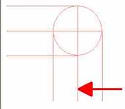
Maybe you expect to receive something like that:
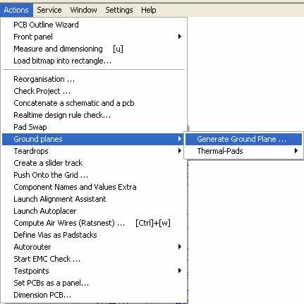
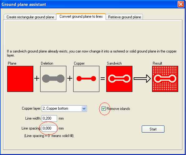
The rub-out of signal islands is done in the "Ground plane as lines" procedure where you can define the line width and the spacing width of a ground plane as grids. Here is a delete signal islands option. Remember to set the line spacing to zero so you will get a solid fill. Sure you can leave it gridded if you like. Please see in menu Actions/Ground planes/ Generate Ground Plane:
and then...
Please note that this procedure should be the very last step of your layout work because further modifications are difficult. For example the "check project" function will check all grid points against all signals. This sure will take a while. So do all design and check actions prior to the ground plane and rub out generation.
Milling tolerances and panel production
Our project board is small (36x38mm) and I would like to know the tolerance you are providing for the outline dimensions.
Beta LAYOUT GmbH (the manufacturer) says +- 0,1mm. Independently from the question how big you draw the outline, the cutting edge always is the middle of this line. The width of the milling tool does not matter in this respect (it's width is recognized in the cutting process).
You may know that we here are the TARGET -people. That means we are the makers of the software TARGET 3001!. We are no PCB manufacturers. We cooperate with the board manufacturing company "PCB-Pool" (= Beta LAYOUT GmbH) located in Germany and Ireland. You can directly calculate the price and order with them from TARGET 3001!. Beta LAYOUT GmbH informs on the routing specifications here:
http://www.pcb-pool.com/download/spezifikation/eng_e_fraesen.pdf
In case you are ordering from out TARGET 3001! with them, you are contracting with them.
Also, it would be nice to know how our final product would look like. If we are going to order a few hundreds of those, would you release them with our final dimensions 36x38mm (not like 20 boards per plate)?
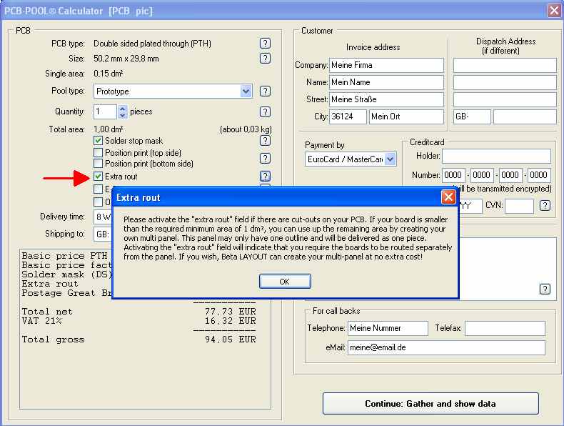
For making sure that you get all boards separated within your own panel, please see in the PCB-Pool calculator (in TARGET 3001!)the following dialog:
Tick "Extra Rout"]]
Click on image to enlarge
Tick the "Extra rout" option (red arrow). What it means, please note in the info box. The good people at Beta LAYOUT GmbH will be pleased if you would get in contact to them to clarify on production issues. phone: ++353 6170 11-0, web: http://www.beta-layout.com
Is it possible create a gridded ground plane and a solid ground plane at same time on the same layer?
I have 2 ground planes on a top of a PCB with different signal name. They are not connected. I have to generate a solid ground plane for one and a gridded ground plane for the other but. I cant because when I generate net ground plane on top TARGET 3001! creates a grid for both.
Yes, it is possible. I made this ones referring to layer 16, copper top.
- define the gridded area first on layer 14 area topin solid by drawing a filled figure upon layer. Give it the signal GND1.
- open Menu Actions/Groundplanes and make it a groundplane using the first tab of the dialog.
- open the same dialog again and make it a grid by using the second tab of the dialog. Make sure having it assigned to layer 16, copper top. You will see the area in grid now.
- now open the big layer dialog by the icon
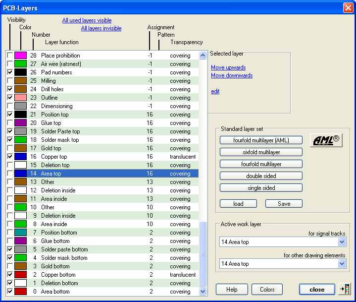
 . You can see that the assignment of layer 14, area top is set to zero. Set it to 16 again.
- now delete the old area definition on layer 14, area top.
- now define the second area for a solid ground plane upon layer 14, area top.
- give it signal GND2 for example
- you're done.
Pads: I want to have some millings for fastening/mounting a heatsink like oblong pads with oblong holes
They shall be about 3 mm long and 1/2 mm wide with a solderable copper area around. Could you please tell me how to design them?
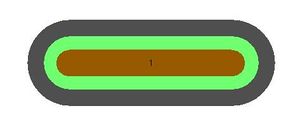
Use a pad from the drawing function (pencil). Set it's width and height to the desired copper-dimension(3 mm long and 1/2 mm wide plus the surrounding copper). Also set Pad-form=oblong and drilling=not wider than 0,5mm. What you get is an oblong pad with a centered drilling of 0,5mm width. Now add a milling of 0,5mm width and 3mm length to the pad. Draw it on layer "25, Milling". Together it comes out that way:
Grey is the aura which is the spacing to other copper elements, defined on deletion layers (top and bottom). Brown is the milling you have defined. It is added to the drillhole ("mills it away"). What you see in green is the soldermask placed upon the copper of the pad. It means: "Here is NO solderstop". Solderstop layers are displayed inverted. Thus: green remains solderable. Each of the elements of this construction idividually can be adjusted. Hover the mouse over the pad and press key [s] for "select" as long as the desired element flashes. Press [Enter] to get it highlighted at last. Now press key [e] for "edit" and enter to the opening dialog. Also see Thermal Pads.
Can I generate mass surfaces upon internal supply situations (multilayer)?
You can provide the individual supply situations with ground, e.g. with the ground plane assistant. Select the appropriate signal, and set the aura to 0 mm, so that it is connected directly with the ground plane. Note: All plated vias, which connect the lower and the upper copper layer, must have an aura of e.g. 0.3 mm, otherwise a short circuit with the ground planes will occur. Therefore use plated-through holes with an adjustment of the aura of more than 0 mm. On 4times multilayer circuit board with ground planes, set the mounting holes (plated-through holes with width and height measurements smaller than the drillhole) with an aura as well. Also check the mounting holes of plug connectors or transistors.
Tracks without soldermask
We are inquiring if it is possible to create tracks with no solder mask. Is this possible? We use Target3001 Version 12.
The soldermask in TARGET 3001! is displayed inverted. That means all areas where no soldermask shall be applied are displayed in green. So if you want to release a piece of track from solderstop varnish, please draw the desired shape on the related solderstop layer. If it appears in green, you can be sure: NO soldermask here.
Is it possible to define cut-off areas in the layout for example to let autoplace only place the digital part of a circuit?
Yes. Set layer 29 to function "place prohibition". Then draw a filled rectangular with the drawing function, to mark a cut-off area on this layer. In this area no packages will be automatically placed. First also make sure that you have only drawn the digital part of your circuit in the schematic, because TARGET will place all package proposals.
All SMD-components are automatically placed upon the lowest layer. How can I place them upon the top copper layer?
This can easily be effected by the use of the "mirror"- function (highlight the component and press key [m] from your keyboard). That's the way how components in general are flipped from the one copper side to the opposite.
How do I create a PCB outline?
You can use the PCB Outline Wizard in the "actions" menu. Draw an outline on layer 23 with the drawing function. With key "POS1" set the relative coordinates to 0/0 (see display in status line bottom left). The cross in hatched lines represents a predefined absolute 0/0.
How can I set the track width in PCB mode once for the entire project?
The width of tracks is determined by two aspects:
1. Minimum width: double click the green signal track in schematic mode, press button properties, set "minimum width=1mm"
2. Standard track width: when signal "minimum width=normal" is set: Left edge of screen, open hierarchy browser, doubleclick "project", click M1 on "project options", then open context menu by M2 and choose "properties". Set "Track width PCB" and "Standard Track width" as required.
You can also set the track width manually. Press key [o] for options when you have the track already started (the thread is fixed to the cursor). If you click the signal after pressing [o] the automatism is activated again.
How do I create a non rectangular ground plane?
- The ground plane can not be created with the ground plane assistant.
- First draw your normal wires eg on layer 2, copper bottom.
- Set the layers "0, Area Bottom", "1, Deletion Bottom" and "2, Copper Bottom " visible. Use the Layers tool and tick all coloured boxes for visibility or press button "all" at the bottom of the list.
- By the use of the drawing function draw the desired geometrical figure upon layer 0, Area Bottom.
- Highlight the whole circuit board with a catch window.
- Press the key "e". The dialog "edit the selected elements" appears.
- Click on " individual dialogs for each element kind" and activate all small boxes (items), which have to be removed out of the area, in which the tracks run in "protected manner" e.g.: Pads, Tracks, Vias...
- Click M2 " individual properties for the selected", and set the " aura " to e.g. 0.3 mm.
- Connect signal "GND" to the ground plane!
- Mark the complete signal GND, and press afterwards the key "E".
- Click Tracks, Vias, "Individual properties for the selected" and Aura.
- Set the aura to 0 mm, afterwards OK.
see also Groundplane
How do I place " text ", e.g. the designation of the circuit board, into a ground area?
Press the key "?" (without shift). Then press M2 and type the appropriate text within "contents" in the dialog . Important: set a "deletion layer". For a ground area on e.g. the bottom copper layer choose layer "1 deletion bottom" in the mentioned dialog.
When placing component packages using the autoplacer, can the orientation be preselected (e.g. place all components horizontally in for later flow soldering)?
Yes. Enter the following parameter into the property list of the respective schematic symbol (M11 on respective symbol) opens dialog "Change symbols". Choose properties-button:
- Set in Properties and value column:
- AUTOPLACER_Rotate 360
the entry 360 means: turning of this component prohibited. the entry 180 means: turning of this component of 180°.
Further entries are ignored as well as the entry of the symbol °. The orientation is determined by how the package-component has been exported (the package will be saved with this orientation). In our library e.g. all DIL-packages are saved horizontally orientated. With entry of "360" in this case, all DIL-packages are to be horizontally orientated (thus turning denied). If you want it to be vertically orientated, you will need to save it vertically orientated.
I have designed a PCB without a schematic and placed the air wires. How can I now remove placed air wires?
Click the soldering pad which the air wire to be removed is connected with a double click. In the following dialog "Change pads" please remove the entry of the signal name. After pressing the OK-button the pad is cut off from the air wire. If this does not work, press buttons [STRG] + [w], to recompute the air wires. If you want to delete the air wire of a special part of your layout first select the desired part with a snap window. Then press button [e]. In the "change elements" dialog, check the "pads" box. Pressing OK in the "change pads" dialog will delete the signal name from the list. NOTE: the hook for "signal" must be set/b>
