Pin
Place a pin when creating a schematic symbol
A pin in TARGET 3001! is the electric connection terminal of a schematic symbol:
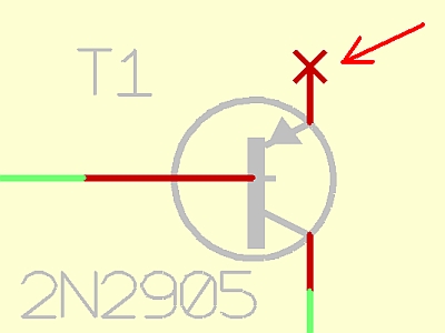
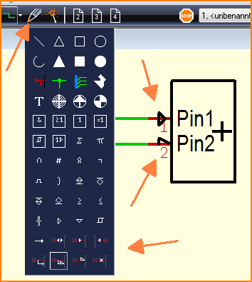
You can reach this mode...
by [1] or
by "Place Pin" in menu "Elements" or
by the icon ![]() .
.
Leave this mode...
by [ESC] or M12
What you can do...
You can place free pins with M1 clicks or by pressing [1] in pointer mode. Free pins are only used when defining new symbols which shall be saved as a component into the component data base. The pin numbers are incremented automatically. Having the phantom image of the pin on your cursor press [o] for Pin Options. This dialog allows settings for the pins about to come. The following options dialog shows some info about the component - and signal assignment. Now place the pins by mouse click. Place the ultimate pin by [Return] or [Esc]. It is possible to change number, form and function of a pin after placement by clicking M11 on it. The dialog "Change pins" will open which is different to the "Pin options" dialog.
In order not to highlight a complete component but only a pin, please release button ![]() in the pointer toolbar before double clicking a pin.
in the pointer toolbar before double clicking a pin.
Pin Options
The pin options dialog opens when pressing key [o] while having selected the "Place pin" mode. It is meant for defining a pin's properties for now and future placements. These placements are meant only for the creation of a new schematic symbol. All other pins you will import to the schematic as part of existing symbols from the component database. Even if a component has only one pin and one pad (C1x1)!
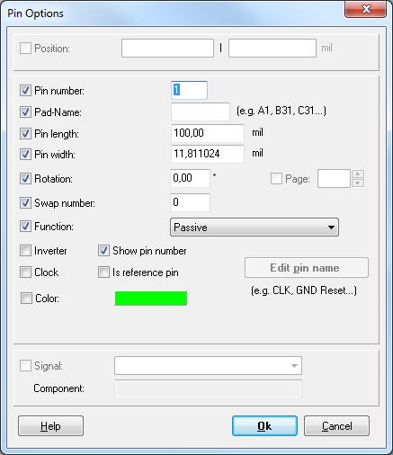
Pin number: The connection between the pin in the schematic and a pad in the package is this number. One of the most important informations a pin carries is the Pin number. Pin names are not regarded.
Pad names like A1-A20 and B1-B20 and C1-C20 are not regarded.
Pin length and width: Represent the hugeness of the red line element.
Rotation: Degree of rotation around the connection cross
Swap number: Pins within the same symbol or gate and with the same Swap number greater than zero can be swapped with this pin.
Function: Defines the function of the pin. Select from the following:
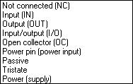
Not connected (NC): Pin is not connected (not used)
Input (IN): Pure Input
Output (OUT): Pure Output
Input/output (I/O): Changing input and output
Open Collector (OC): open collector output (open drain)
Power pin (Power input): Power supply of a component
Passiv: Pin of a passive element or function not clearly defined
3 States(Tristate): Output, which can achieve high-Ohm-impedance
Power (supply): Power supply of a PCB e.g. a connector supplying power to the PCB.
Or the output of a voltage controller (e.g. 7805) which supplies others
Power pin means that this is a pin that needs power.
Power (supply) means that this pin gives power. Normally a connector pin is set to
Power (supply). Power comes through this pin onto the PCB. Also pin 2 of a 7805 is a power supply pin.
It supplies the other ICs with power. Their Power pins are consumer pins.
Inverter: The pin gets an inverter point.
Clock: A little arrow shows that this pin is a clock input.
Show pin number: Shall the pin number be visible? Useless for resistors, useful for ICs.
Is reference pin: If this box is checked, the pin is not representing a pad in PCB but is a signal reference pin such as used for ground symbols. This box shall only be used, when creating reference symbols.
Color: Define color of a pin independently of predefined color. Is color white (R=255, G=255, B=255) chosen, the predefined standard-color is used. If you wish color white although, you need minimal offset from the above mentioned RGB characters (just one point fits).
Edit pin name: The dialog for the pin name will be opened.
Pin Look
There are several symbols that can be added to a pin:
Change Pins
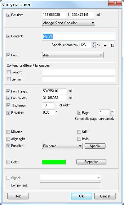
The "Change Pins" dialog opens after M11 ohn a pin with the intension to change it. The dialog looks similar to the "Options" dialog but the entries refer only to this singular editing action.
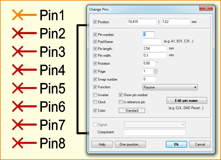
Position: Shows absolute coordinates.
Other functions as above.
A name is generated while creating a pin. This name can be selected separately to be renamed or moved. If for the logic of the circuit you only need the name of the pin but not the pin number please change the name and then delete it by M1 and [Delete]. It will remain invisible.
Pin Swap
You can reach this mode...
by "Pin Swap" or in menu "Actions" or
by the tools ![]() .
.
Leave this mode...
by [ESC] or M12
What you can do...
Click the two pins or pads of the same symbol subsequently with M1. Both pins have to have the same non-zero swap number. In the schematic only the two pin numbers are exchanged. In the PCB the connected tracks are dragged along like rubber tracks. Caution: Short cuts are possible.
Pin name
The pin name is the Text concerning a connection pin in the schematic showing its function e.g. GND or CLK or RES. Contrarily to the pin number it is a real individual data element in TARGET 3001!. It is placed or edited by a double click M11 on the Pin in question. The opening dialog is named: "Change Pins", see above. In this dialog please find button "Edit pin name" used to open the following dialog:
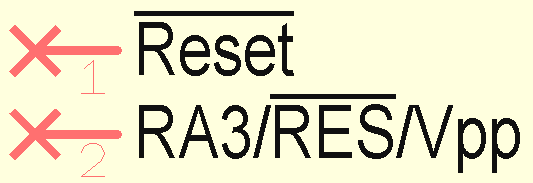
The pin name can also have an overbar. The pin name in the editor starts with a vertical bar (tube) then |. For example |Reset. The complete pin name has an overbar then. The overbar can also start within the pin name or end there: RA3/|RES|/Vpp. In the middle of the pin name has the word RES an overbar. Only one overbar can be used within a pin name.
Don't mix up pin name and pad name which is a alphanumerical naming of pads arranged like a matrix e.g. in BGAs or connectors (A1, A2, ... B1, B2, ... B31). Thus a Pin additionally to its Pin name can have an alphanumerical Pad name which will be displayed in schematic and layout instead of the Pin/Pad number. The Pin number nevertheless internally is kept as the internal link between pin and pad.
Edit selected pin names in a text editor
Please find this option in schematic menu "Components". It is meant for the edition of the texts of pin names in a bunch of pins highlighted. This little text editor is able to receive the contents of your clipboard; maybe copied from a PDF datasheet. So it is easy to letter a number of pins at the same time.
The lettering of numerous free pins
If you want to draw a new schematic symbol you may act the way to place the number of pins required just the way they come on a free space in the schematic. Now open the menu option "Edit selected pin names in a text editor" in menu "Components".
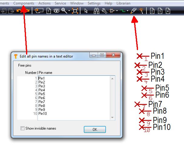
Image: 10 free pins placed and dialog opened for edition
In the dialog you see the row of pin numbers in the column to the left. In the text area right beside the pin names are listed. They all together now can be edited.
TIP: Copy the pin names of your desired symbol from the PDF data sheet to your clipboard and paste them here to this text area. Now move each name to the matching row representing the pin number - done.
Edit pin names of a symbol in a schematic
In a existing schematic highlight a complete symbol and now use the menu option "Edit selected pin names in a text editor" from menu "Components". The opening editor now lists all pins from the highlighted symbol and allows the edition of their names. Again you may paste contents of your clipboard here.
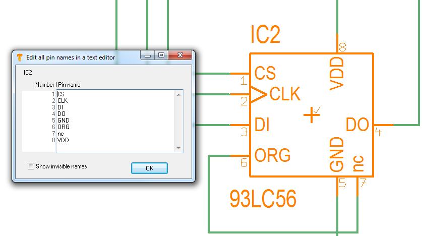
Image: Edit pin names of an existing schematic symbol
Show invisible names: A pin name can be invisible if you had deleted it. If you had done so with this component, you can fade in deleted pin names now. This makes sense during the pin name edition. Later in schematic you may delete them again.
Draw a new schematic symbol quick and easy by the use of your clipboard
Say in TARGET 3001! you would miss the component QT60240
www.atmel.com/Images/qt60240_r8.06.pdf
Fist take a short look at the package...
From the data sheet you can see that it uses a MLF-32 package. This package is available in TARGET 3001!.
If in your case the package might not be available, please create it using the Package Generator.
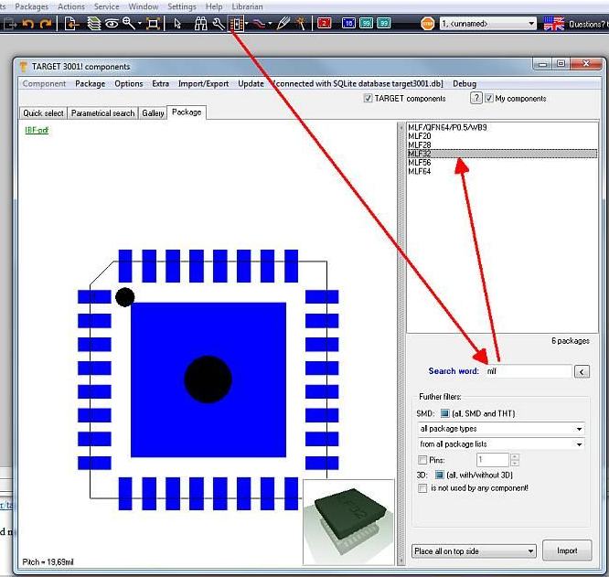
Image: Find the mlf32 package using the package browser
Regarding the schematic symbol now leave this dialog and just place 32 pins anywhere to a free place in an empty schematic. Use the pin symbol under the "pencil icon" and repeatedly place pins so that they get consecutive numbers.
Now open the data sheet and take the pin names to your clipboard:
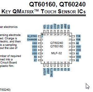
Image: Excerpt of the data sheet: www.atmel.com/Images/qt60240_r8.06.pdf
Now go back to your schematic and open menu...
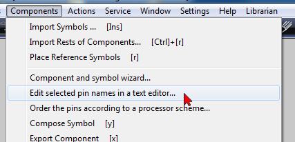
Image:
....and paste the names to the inner of the text area. Outer of the text area to the left you see the column of your 32 pin numbers which you just have placed to the schematic (TARGET recognizes them automatically because they are free).
Now bring the names to the right order. If some of them are upside down in a bunch, mark them and use the "Revert" button:
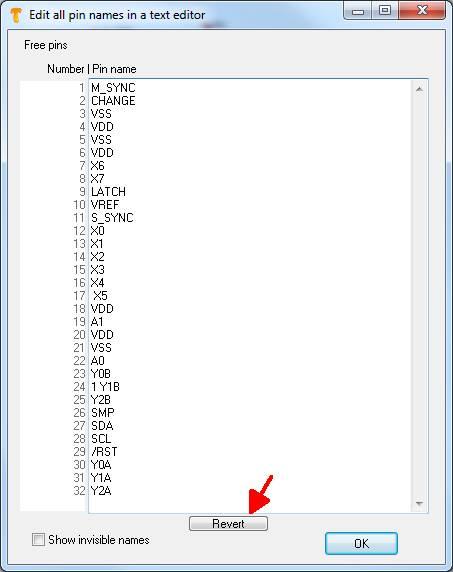
Image:
After OK you will have all names brought to the pins in the right order. Now press OK to close this dialog. Draw an open rectangle for the body of the symbol and assort the pins. Give each Pin a double click in order to define its function (Input/Output/Power... whatever) according to the wiring list:
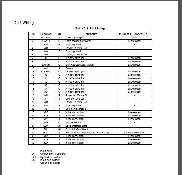
Image:
After you have done this for each of the 32 pins, highlight all and place the cursor to Pin #1. Press key [x] for exporting it to the data base. Give it a name and assign the MLF32 package to it.
Arrange pins according to processor scheme
Say you would have assigned the pin names by the use of the text function and you would have the following image:
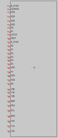
Image:A row of named pins. Not really comfortable to wire...
You might find this row not convenient in respect to wiring it easily and clearly in your schematic. Now use the option "Order the pins in a processor scheme" in menu "Components". TARGET 3001! by this means will arrange the pins as follows:
To the north of your symbol you should have all pins representing supply voltage (+) which means Pin names VDD, VCC, and VPP. TARGET sets their function to power.
To the south of your symbol you should have all pins representing supply voltage (-) which means Pin names VSS or GND.
TARGET sets their function to power.
To the east of your symbol you should have all pins wit a number at the end. TARGET assumes them to be I/O ports. So they get the pin function Input/Output (I/O).
To the west of your symbol you should have all other pins. Here you should individually check and set the pin function accordingly
After using this function your huge symbol comes along smaller and it looks like this:
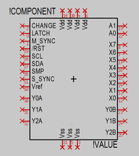
Image:Pins brought to position according to processor scheme. This is more comfortable to wire. Sure you can still move and edit each pin according to your wishes.
Afterwards highlight all and export it to the data base. During this process assign the package MLF-32 to it.
